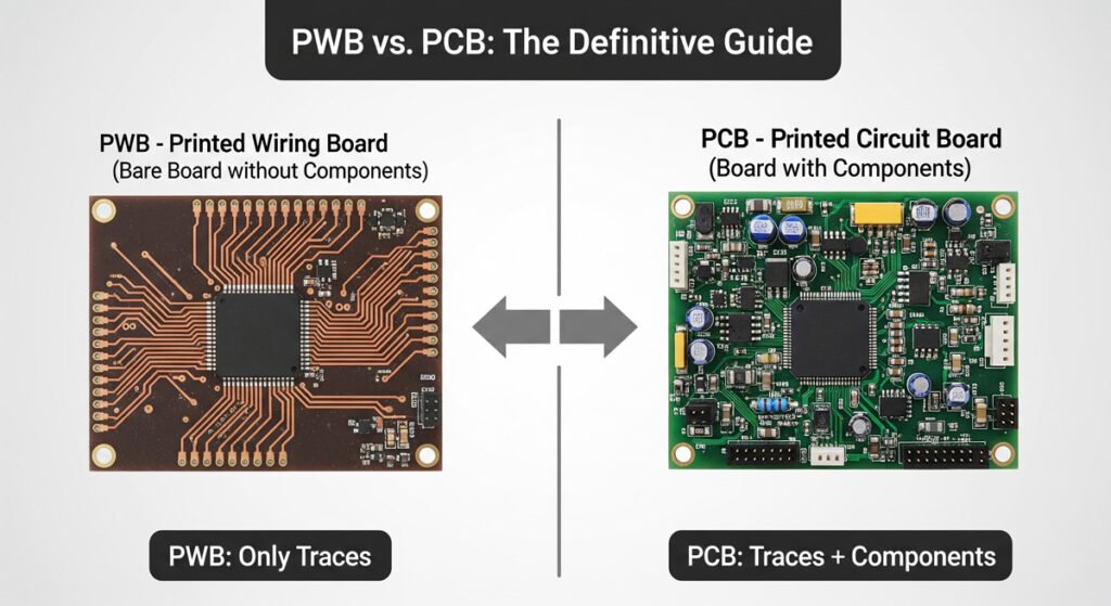
PWB vs. PCB: The Definitive Guide
The terms Printed Wiring Board (PWB) and Printed Circuit Board (PCB) are often used interchangeably, leading to confusion for both hobbyists and professionals. This interactive guide aims to clarify the differences, explore the technical nuances, and help you decide which is right for your project. We'll go beyond simple definitions to provide a practical and actionable understanding.
The Core Debate: Three Meanings
This confusion is more than just a matter of semantics; it stems from historical evolution, modern manufacturing practices, and regional preferences. Understanding these three contexts is key to unraveling the mystery.
1. The Historical Distinction
Originally, the PWB was the precursor to the modern PCB. It was a simple board with etched conductive paths or "wires" to connect electronic components. The term PCB emerged as technology advanced and boards began to carry more functionality, forming a true "circuit." The PWB is its ancestor, focused on pure point-to-point connections.
2. The Modern Distinction
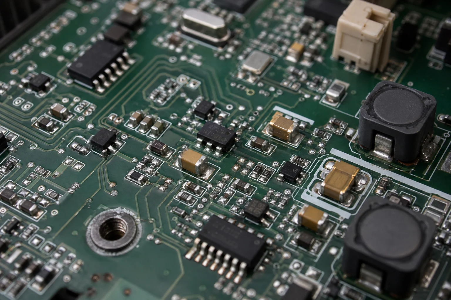
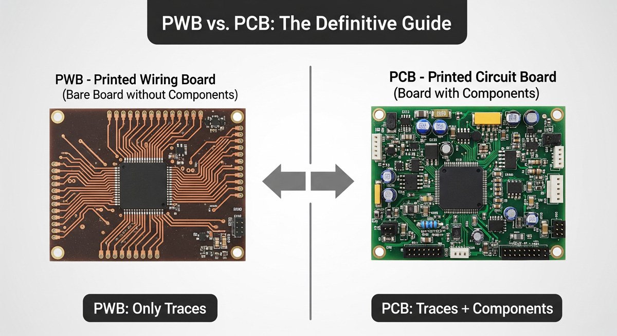
In today's manufacturing world, the terms often describe different stages of completion. PWB is commonly understood as the "bare board" - the raw, unpopulated board with only the conductive traces. It becomes a PCB once electronic components (like resistors, ICs, capacitors) are soldered onto it. This distinction is crucial for clear communication in the supply chain and assembly process.
3. The Regional Nuance
Regional differences also play a role. In Japan, the term PWB is preferred to avoid confusion with the acronym for polychlorinated biphenyls, a toxic chemical. Additionally, in highly regulated industries like aerospace and military, PWB is sometimes used precisely to refer to a bare board to ensure absolute clarity of terms.
Feature-by-Feature Comparison
While often used interchangeably, PWBs and PCBs have notable technical differences. Select a feature below to view a visual comparison and detailed explanation.
Which One Do You Need?
Your choice depends entirely on your project's needs. Are you a hobbyist experimenting with a simple circuit or an engineer designing a high-performance device? Select the role that best fits you for tailored advice.
Electronics Hobbyist / Student
Working on a DIY project or learning the basics.
Design Engineer
Designing for performance, reliability, and mass production.
Procurement Specialist
Focused on cost, manufacturing, and supply chain.
Beyond the Acronyms
The world of electronics is full of abbreviations. Here's a quick guide to related terms to give you a complete understanding.