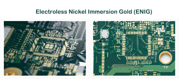
ENIG Surface Finish: PCB Design Guide
ENIG (Electroless Nickel Immersion Gold) basics: thickness, pros/cons, and applications. Learn to specify ENIG for lead-free PCBs. Best practices inside!

ENIG (Electroless Nickel Immersion Gold) basics: thickness, pros/cons, and applications. Learn to specify ENIG for lead-free PCBs. Best practices inside!
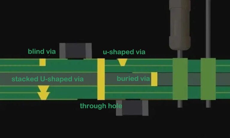
Learn via types: through-hole, blind, buried, and vias-in-pad. Tips for spacing, drilling, and reliability in multi-layer PCBs. Essential for advanced layouts. Guide inside!
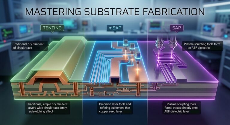
A technical comparison of Tenting, mSAP, and SAP processes in high-end PCB substrate fabrication. Explore how these methods solve side-etching issues and enable sub-10μm line precision for AI and 5G chips.

With the continuous deterioration of urban air quality, the air purifier in the car has become a hot-selling product in the automotive supplies. This article introduces our reverse design case of a car air purifier. Reverse Design of Car Air

New to pinouts? Learn how to read component pin configurations, avoid connection errors, and map signals to PCBs. Essential for beginners and engineers. Start here!
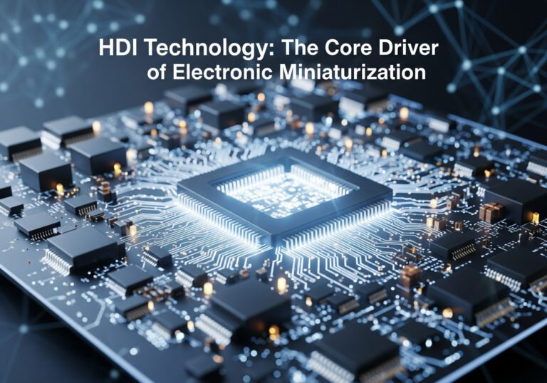
In the rapidly evolving world of electronics, the push for miniaturization is a constant. From powerful smartphones to compact wearables, the demand for smaller, more functional devices is ever-increasing. This trend has placed immense pressure on engineers to pack more
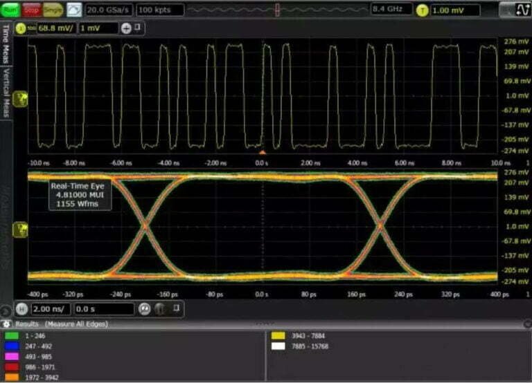
Master SI issues: reflections, crosstalk, and impedance control. Tips for routing, termination, and simulation tools like HyperLynx. Critical for high-speed designs!
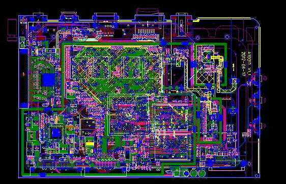
What is 6-Layer PCB Manufacturing? 6-layer PCB manufacturing is the mass-production of PCBs with a minimum of six layers. In a 6-layer PCB, the top and bottom layers are usually made of laminated material which is then covered with a