Optical computing is developing rapidly in the field of AI and has broad application prospects. Recently, the semiconductor research team of the Chinese Academy of Sciences developed an ultra-highly integrated optical convolution processor. This marks a major breakthrough in the field of optical computing in China.
A few days ago, the Chinese Academy of Sciences announced that the team of researcher Li Ming and academician Zhu Ninghua from the Microwave Optoelectronics Research Group of the State Key Laboratory of Integrated Optoelectronics, Institute of Semiconductors, Chinese Academy of Sciences, has developed an ultra-highly integrated optical convolution processor. The relevant research results were published in “Nature-Communications” under the title of “Compact optical convolution processing unit based on multimode interference”.
Introduction to Optical Convolution Processor
Convolutional neural network is an artificial neural network inspired by the biological visual nervous system. It consists of multiple layers of convolutional, pooling and fully connected layers. As the core component of the convolutional neural network, the convolutional layer extracts features of different levels and abstraction levels through local perception and weight sharing of the input data. In a complete convolutional neural network, the computation of convolution operation usually accounts for more than 80% of the computation of the entire network. While convolutional neural networks have been successful in areas such as image recognition, they also face challenges. The traditional convolutional neural network is mainly based on the electrical hardware implementation of the von Neumann architecture. The storage unit and the processing unit are separated, resulting in an inherent contradiction between data exchange speed and energy consumption. With the increase of data volume and network complexity, it is increasingly difficult for electronic computing solutions to meet the demand for high-speed, low-power computing hardware for real-time processing of massive data.
Optical computing is a technology that uses light waves as a carrier for information processing. It has the advantages of large bandwidth, low latency, and low power consumption. The problem of tidal transport of data in the Neumann computing paradigm. Optical computing has attracted much attention in recent years, but in most of the reported optical computing schemes, the number of optical elements increases quadratically with the size of the computing matrix, which makes the scaling of optical computing chips a challenge.
Research results of the optical convolution processor
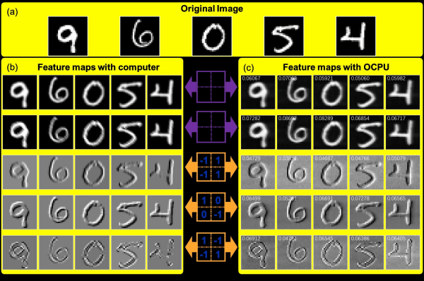
The optical convolution processing unit proposed by Ming Li-Ning-Hua Zhu’s team constructs three 2×2 correlated real-valued convolution kernels through two 4×4 multimode interference couplers and four phase shifters (Figure 1). The team innovatively combines the wavelength division multiplexing technique with the multimode interference of light to characterize the Kernel elements in terms of wavelength, the input-to-output mapping realizes the multiplication operation process in convolution, the wavelength division multiplexing and photoelectric conversion realizes the addition operation in convolution, and the related convolution kernel reconfiguration is realized by adjusting the four thermal tuning phase shifters (Figure 2).


The optical convolution processing unit proposed by the team experimentally verifies the feature extraction and classification capability of handwritten digital images. The results show that the image feature extraction accuracy reaches 5 bit; the accuracy of handwritten digits from the MNIST handwritten digit database is 92.17% by ten classes. Compared with other optical computing schemes, this scheme has the following advantages: (1) high arithmetic density: combining optical wavelength division multiplexing technology with optical multimode interference technology, four modulation units are used to realize three 2×2 real-valued Kernel parallel operations, and the arithmetic density reaches 12.74-T MACs/s/mm2. (2) linear scalability: the number of modulation units grows linearly with the matrix size, which has very strong potential for large-scale integration.
Advantages and Applications of Optical Chips
Companies represented by Lightmatter and Lightelligence have launched a new type of silicon optical computing chip, which far exceeds the performance of the current AI computing chip. According to Lightmatter’s data, the Envise chip they launched runs 1.5 to 10 times faster than Nvidia’s A100 chip. times.
The laser chip and the detector chip are collectively referred to as an optical chip. The optical chip is the basic component for realizing photoelectric signal conversion, and its performance determines the transmission efficiency of the optical communication system. Compared with traditional optical components, optical chips have the advantages of small size, light weight, low power consumption, and high integration, and can realize high-speed, high-precision, and high-reliability optical signal processing and transmission. In the context of massive growth in computing power infrastructure construction, optical chips will usher in huge opportunities.
As the transmission rate increases, the proportion of optical chips in the cost of optical modules is also increasing. Optical chips account for 30% of optical modules below 10Gbs, 40% of 10Gbs-25Gbs optical modules, and 40% of optical modules above 25Gbs Zhongguang chips accounted for 60%.
Optical modules are currently mainly used in the field of optical communications. According to LightCounting data, the global optical module market will grow by 14% year-on-year in 2022. It is estimated that the CAGR of the global optical module market will be 10% from 2022 to 2027, and will exceed US$20 billion in 2027.
Demand Analysis of Optical Chip Industry Chain
Optical chip development is inseparable from optical communication and optical module, and the industry is in an accelerated development stage. Optical chips are an important part of optical communication and optical modules, and with the development of the optical communication industry and changes in application scenarios, both optical modules and optical chips are accelerating their development. The optical module industry has experienced decades of development, and the initial formation of the industrial system of photonic integration technology has driven the rapid development of the optical chip industry Optical chips play an important role in reducing fiber loss and other aspects, and have great potential for development in emerging areas.
And from the perspective of the entire optical communication industry chain, optical chips and electrical chips, structural components, auxiliary materials, etc. constitute the upstream of the optical communication industry, the midstream of the industry for optical devices, including optical components and optical modules, the downstream of the industry assembled into system equipment, and ultimately used in the telecommunications market, such as fiber optic access, 4G/5G mobile communication networks, cloud computing, Internet vendors data centers and other fields.
As the demand for optical communication grows, the demand for optical communication chips is growing rapidly. ICC estimates that China’s high speed rate optical chip market space is expected to reach USD 3.022 billion in 2023 and USD 4.34 billion in 2025. Meanwhile, China’s share in the global optical communication chip market is expected to continue to rise.
At present, a new round of technology revolution represented by AI is sweeping the world, and ChatGPT developed by OpenAI makes AIGC attract much attention. In the context of the accelerated commercialization of AIGC applications, the massive growth and upgrade of arithmetic infrastructure will become an inevitable trend. Under the background of arithmetic infrastructure construction, optical chip is expected to usher in a new round of growth opportunities.
In terms of specific applications, the arithmetic requirements of AIGC give rise to the demand for high speed and large bandwidth networks, and the evolution of optical modules to higher speed will strongly promote the technological upgrade and replacement of optical chips. At the same time, the network architecture upgrade of data centers has led to an increase in internal optical connections, and the traditional three-layer architecture of data centers is transitioning to a leaf spine architecture, which means that optical modules need faster transmission rates and higher coverage rates, and mid- to high-end optical chips are expected to rapidly expand. The rapid implementation of LIDAR and other applications will also strongly boost the demand for optical chips.
The Development Landscape of Optical Chips in China
While Europe and the United States are leading in optical chip technology, Chinese optical chip companies are also catching up, and the global market is currently dominated by the United States, China and Japan. Global optical chip companies have formed a closed-loop industry and high industry barriers, and can independently complete key processes such as chip design, wafer epitaxy, and mass production of optical chips with 25G and higher rates. Some Chinese optical chip companies already have the leading level, and their competitiveness will be further enhanced with the improvement of technical capability and market recognition.
After years of development, China’s various types of optical chips are developing rapidly, and the specific pattern is as follows:
- 2.5G and below optical chips: mainly used in fiber access market, domestic optical chip companies have occupied the main market share.
- 10G optical chips: mainly used in fiber access market, mobile communication network market and data center market. China’s optical chip companies have basically mastered the core technology of 10G optical chip, but some models still have a high technical threshold and rely on imports.
- 25G and above optical chips: mainly used in the mobile communication network market and data center market, including 25G, 50G, 100G laser and detector chips.
Nevertheless, China’s demand for high speed optical chips is high. 25G and above rates belong to high speed optical chips, currently dominated by leading companies in Europe, America and Japan, Oclaro, Avago, NeoPhotonics, etc. have 50G EML chip capability, DFB and VCSEL laser chips have reached the highest rate of 50G for large-scale commercial use, Finisar, AAOI, Oclaro have 50G EML chip capability, AAOI and Oclaro have the capability of 50G PAM4 DML chip, and there is a gap between China and the leading level of overseas industries.
The good thing is that the main application scenarios of optical chips include fiber optic access, 4G/5G mobile communication networks, data centers, etc., are in the key window period of rate upgrade and generational change, in the context of the rising demand for high-speed transmission, the proportion of optical chips used in the future 25G rate optical modules will gradually expand, and by 2025, the overall market space will reach $4.340 billion, with a compound annual growth rate of 21.40%. Growth rate will reach 21.40%, Chinese manufacturers in the field of high-speed optical chip is expected to achieve self-sufficiency through their own technical strength.
Conclusion
The optical convolution processor focuses on the field of optical computing, which is a technology that uses optical devices and optical phenomena for information processing and computing. Optics can process multiple pieces of information simultaneously, thus enabling efficient parallel computing. With the development of artificial intelligence, optical computing technology can apply the training acceleration of deep neural network, optical neural network, optical logic gate and so on.
With the continuous development of artificial intelligence technology, the requirements for computing speed and efficiency are getting higher and higher. Optical computing chips can provide a solution with high efficiency and low energy consumption, and are expected to become an important part of the future artificial intelligence industry.


