What is NRF51822 BLE Chip?
The nRF51822 is a powerful, flexible, multi-protocol SoC ideal for Bluetooth low energy and 2.4GHz ultra-low energy wireless applications. It is built on a 32-bit ARM® Cortex™ M0 CPU with 256kB flash + 16kB RAM. The embedded 2.4GHz transceiver supports Bluetooth Low Energy and 2.4GHz operation, where the 2.4GHz mode is wirelessly compatible with Nordic Semiconductor’s nRF24L family of products.
Features of NRF51822
- Single-chip, high-flexibility, 2.4GHz multi-protocol device;
- 32-bit ARM Cortex M0 CPU core;
- 256KB flash 16KB RAM;
- Supports S110 Bluetooth Low Energy protocol stack;
- S110 requires 80 kB of memory space;
- Thread safety and runtime protection;
- Event-driven API;
- Wireless Compatible with nRF24L Series;
- 3 data rates (2Mbps/1Mbps/250kbps);
- +4dBm output power;
- -92.5dBm sensitivity, Bluetooth low energy;
- Configurable I/O mapping for analog and digital I/O;
- PPI system for maximizing energy efficiency applications and code simplification;
- Flexible energy management system with automatic energy management for each peripheral product;
Pinout of nRF51822
The nRF51822 pinout consists of 36 pins, and each pin has a specific function. The pins can be divided into four main categories: GPIO, ADC, I2C, and PWM. The GPIO pins can be used for digital I/O and can be configured as either an input or output. The ADC pins can be used for analog input, and the I2C and PWM pins can be used for communication and PWM control.

In addition to the pins mentioned above, the nRF51822 also has two reset pins, two Chip Enable pins, two VTREF pins, four Power Supply pins, and a few other pins. The reset pins are used to reset the device, the Chip Enable pins are used to activate the device, and the VTREF pins are used for analog reference voltage.
How to Program NRF51822?
Programming the NRF51822 ble is a little complex task, below are steps.
Environment Building and GPIO usage
Step 1. Development Tools
The following tools are required:

Step 2. Development Environment Building
Create a new folder, where component is the decompressed file of the SDK compressed package. Inside the config file is the sdk_config.h file, which is copied from the examples in the SDK. Users is the folder where the MDK project is stored.

Open the MDK and pack installer. Then search and select the nRF51822 chip to install the necessory packs.
As shown in the figure, select the CORE file and the Startup file.

Step 3. Writing GPIO Program
There is a detailed introduction to GPIO in the nrf_gpio.h library file, and several main functions are listed below.
					//input Output
typedef enum
{
     NRF_GPIO_PIN_DIR_INPUT = GPIO_PIN_CNF_DIR_Input, ///< Input.
     NRF_GPIO_PIN_DIR_OUTPUT = GPIO_PIN_CNF_DIR_Output ///< Output.
} nrf_gpio_pin_dir_t;

// pull up and pull down
typedef enum
{
     NRF_GPIO_PIN_NOPULL = GPIO_PIN_CNF_PULL_Disabled, ///< Pin pull-up resistor disabled.
     NRF_GPIO_PIN_PULLDOWN = GPIO_PIN_CNF_PULL_Pulldown, ///< Pin pull-down resistor enabled.
     NRF_GPIO_PIN_PULLUP = GPIO_PIN_CNF_PULL_Pullup, ///< Pin pull-up resistor enabled.
} nrf_gpio_pin_pull_t;

//Input and output initialization configuration
void nrf_gpio_cfg_output(uint32_t pin_number);
void nrf_gpio_cfg_input(uint32_t pin_number, nrf_gpio_pin_pull_t pull_config);

//Output high and low/flip level
void nrf_gpio_pin_set(uint32_t pin_number);
void nrf_gpio_pin_clear(uint32_t pin_number);
void nrf_gpio_pin_toggle(uint32_t pin_number);

// read input and output levels
uint32_t nrf_gpio_pin_read(uint32_t pin_number);
uint32_t nrf_gpio_pin_out_read(uint32_t pin_number);
Next, we need to define the LED location on Pin. According to the schematic diagram of nRF51822, the P0.07 pin is connected to the LED.
					#include "nrf_delay.h"
#include "nrf_gpio.h"

#define LED 7

int main(){

   nrf_gpio_cfg_output(LED);

   nrf_gpio_pin_clear(LED); //Output low level

   while (1) {


     nrf_gpio_pin_toggle(LED); // flip level

     nrf_delay_ms(1000);


   }
}
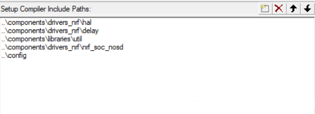
After writing the above codes, you will find there’s a compilation error because the header file path is not found. So we should import the header file path, as shown below:
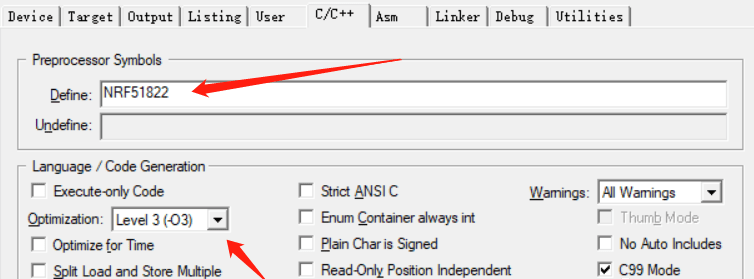
And then set the macro definition, as shown below:
Step 4. Download the Program
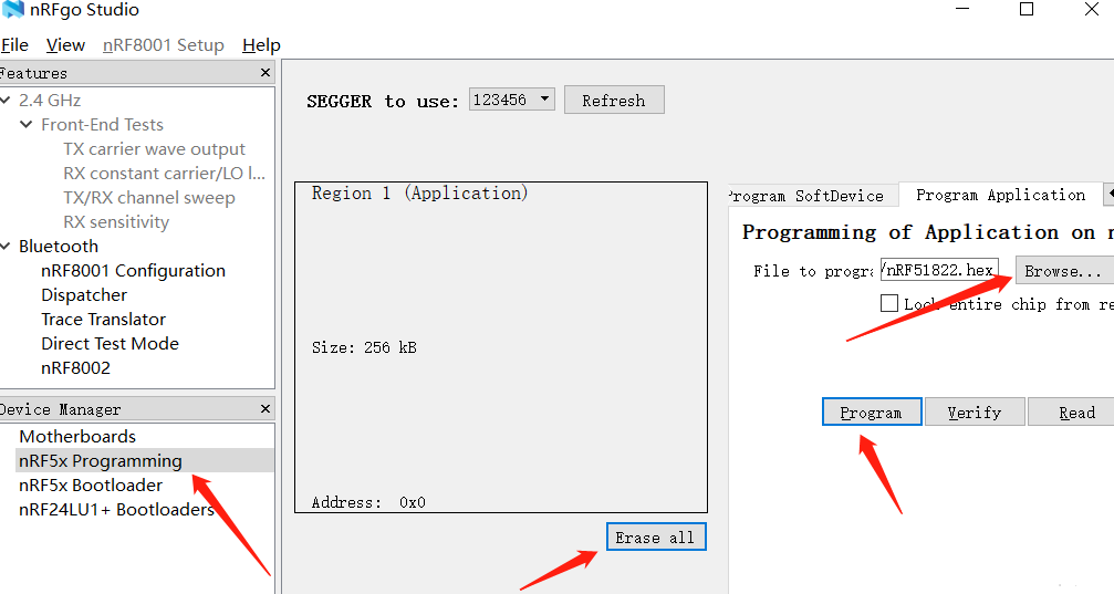
Connect the development board and PC by J-Link’s SW method, and open nRFgo Studio.
- Click nRF5x Programming;
- Click Erase all to clear the memory;
- Select the hex file;
- Programming the nRF5x and download.
Applications of nRF51822
- Bluetooth Smart App;
- Mobile phone accessories;
- Computer peripherals;
- Smart home appliances: fitness and healthcare sensor;
- Electronic games Controller;
- Approach and Safety Alert Systems;
- Home/Industrial Control and Data Acquisition;
- Intelligent RF Tracking and Social Interaction;
- Remote controls for TVs, set-top boxes and media systems;
NRF51822 vs NRF51802
In addition, for the NRF51802 chip of the same series as the NRF51822, the FLASH RAM capacity of these two chips is the same. The difference is that there are slight differences in sensitivity, power consumption, standby current and internal wake-up time. The comprehensive data displayed by the 51822 is better. Usually, The two models are interchangeable.
At present, our company has realized the reverse analysis, decryption and analysis optimization of NRF51822 and NRF51802 Bluetooth chips.


