Practical Challenges in PCB Reverse Engineering and Rework
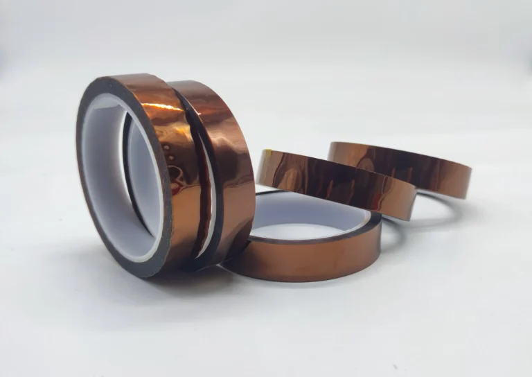
In PCB reverse engineering and rework, masking and thermal control are rarely treated as minor details. Engineers routinely apply kapton tape on PCB assemblies to protect sensitive areas during component removal, inspection, and reassembly. Whether it is shielding gold fingers from heat or isolating adjacent traces during rework, polyimide tape for PCB masking has become a practical necessity rather than a specialized option.
Unlike controlled production environments, reverse engineering often involves repeated heating cycles, manual soldering, and localized thermal exposure. Under these conditions, material choices directly affect process reliability. Using the wrong masking material can lead to lifted pads, damaged solder masks, or conductive residue. This is why PCB Kapton tape is commonly seen on workbenches where precision and repeatability matter.
Rather than serving as a simple cover, kapton tape PCB applications function as part of the process itself, helping engineers manage heat, maintain electrical isolation, and reduce the risk of unintended damage during complex rework tasks.
Thermal and Masking Issues in Real-World PCB Workflows
Localized Heat During Soldering and Component Removal
Hot air rework tools, soldering irons, and infrared heaters are essential in reverse engineering, but they introduce concentrated heat that can quickly spread beyond the target area. Nearby components may experience thermal stress, while thin copper traces can warp or delaminate if exposed for too long.
Applying polyimide tape for PCB masking allows engineers to define clear thermal boundaries. Because the material remains stable at elevated temperatures, it does not soften or shift during heating. As a result, kapton tape on PCB surfaces helps confine heat to specific regions, especially when working near connectors, fine-pitch components, or exposed edge fingers.
Masking Demands in Dense and Multilayer Boards
Modern PCBs often combine multilayer stackups with tight trace spacing and mixed surface finishes. These designs leave little tolerance for masking errors. Conventional tapes may deform under heat or leave adhesive residue that interferes with electrical performance.
Kapton tapes for masking PCBs offer both dimensional stability and precise placement. Engineers commonly rely on PCB Kapton tape to protect sensitive traces, vias, and surface finishes during partial disassembly or inspection. In reverse engineering scenarios, this level of control helps preserve board integrity while enabling accurate analysis and testing.
Why Polyimide Tape Is a Standard Tool in PCB Processes
Thermal Stability and Dimensional Consistency
The widespread use of Kapton tape in PCB work is largely driven by its material properties. Polyimide film combined with silicone adhesive provides consistent performance during high-temperature operations. In practical terms, kapton tape PCB use can tolerate temperatures around 260 °C without shrinking or curling, even during repeated heating cycles.
This stability is critical during rework. When masking materials shift or degrade under heat, protected areas become exposed. PCB Kapton tape maintains its position, allowing engineers to focus on the task rather than compensating for material failure.
Electrical Insulation and Chemical Resistance
Beyond thermal performance, polyimide tape for PCB masking also provides reliable electrical insulation. When placed over exposed conductors or adjacent traces, it helps prevent accidental shorts during probing, soldering, or powered testing.
Chemical resistance further supports its use. Flux residues are often removed using solvents such as IPA, and kapton tape on PCB assemblies resists these chemicals without degrading or releasing adhesive. In ESD-sensitive environments, some teams choose ESD Kapton tape to reduce static buildup during tape removal, adding an extra layer of process control where required.
Practical Applications of Kapton Tape in PCB Reverse Engineering and Assembly
Case 1: Protecting Gold Fingers During Connector Rework
In PCB reverse engineering projects carried out in the United States, edge connectors and gold fingers are frequently exposed during inspection or signal tracing, especially on industrial control and automation boards.
In one controller board teardown, engineers needed to remove a nearby power connector to analyze routing paths. Initial rework attempts without masking resulted in slight discoloration along the gold-plated edge, caused by reflected heat during hot-air removal.
Applying kapton tape on PCB edge contacts before rework immediately reduced thermal exposure. The tape acted as a localized heat barrier while maintaining dimensional stability throughout repeated heating cycles. After removal, the contact surface remained clean, with no adhesive transfer—an outcome that would have been difficult to achieve using lower-temperature masking materials.
This example illustrates why polyimide tape for PCB masking is commonly adopted in U.S.-based reverse engineering labs where process repeatability and documentation accuracy are critical.
Case 2 : Isolating Fine Traces During Selective Component Removal
In reverse engineering work conducted in China, engineers often face densely routed multilayer PCBs used in power electronics and consumer devices, where selective component removal is required without disturbing surrounding circuitry.
During a multilayer board analysis, engineers used PCB Kapton tape to isolate adjacent signal traces while desoldering a QFN device. The masking prevented solder splash and limited heat spread to nearby areas. Throughout the process, the tape remained stable and did not shift or deform.
This controlled masking approach allowed clean component removal while preserving trace geometry for subsequent inspection and reverse mapping—demonstrating how kapton tape on PCB assemblies supports precision work in high-density designs.
Case 3: Fixing Thermocouples for Thermal Profiling
In Taiwan, where PCB assembly and validation work often involves close collaboration between design and manufacturing teams, thermal profiling is routinely used to evaluate solder behavior during reassembly and diagnostic testing.
In one profiling setup, thermocouples needed to be temporarily fixed close to pads and component leads. Engineers selected kapton tape PCB solutions to secure the sensors due to the tape’s low thermal mass and high temperature tolerance. The tape held the thermocouples in place throughout repeated heating cycles without influencing local temperature readings.
This practice is common in Taiwanese PCB workflows, where kapton tape on PCB surfaces is treated as a standard tool for measurement support rather than a simple masking accessory.
Comparing Kapton Tape with Other Masking Options Used in PCB Work
Not all high-temperature tapes behave the same in PCB environments. The table below reflects practical differences observed during PCB rework and reverse engineering.
| Property | Kapton (Silicone Adhesive) | PET Silicone Tape | Kapton (Acrylic Adhesive) |
|---|---|---|---|
| Continuous Temperature | ~260 °C | 130–150 °C | ~155°C |
| Adhesive Stability | Excellent | Moderate | Lower at high temp |
| Residue Risk | Low | Medium | Higher after heat |
| Dimensional Stability | Excellent | Moderate | Good |
| Typical Use | Reflow, rework, gold finger protection | Low-temp masking | General insulation |
While PET silicone tapes may appear suitable for masking, they often soften or lose adhesion during extended heating. Acrylic-based Kapton tapes offer higher temperature tolerance than PET, but they are more prone to residue after repeated thermal cycles.
For demanding PCB processes, kapton tapes for masking PCBs with silicone adhesive remain the most reliable choice.
Best Practices That Matter in Daily PCB Work Application and Removal
Application and Removal
To reduce residue risk, apply polyimide tape for PCB masking to clean, dry surfaces and avoid excessive pressure. Removing the tape at a shallow angle while the board is still warm often improves results.
Residue issues are usually linked to adhesive degradation under extreme heat or expired shelf life—not inherent flaws in PCB Kapton tape.
ESD Awareness
Standard Kapton tape is sufficient for most PCB tasks. In ESD-sensitive environments, ESD Kapton tape may be used to reduce static buildup during handling and removal, particularly around sensitive ICs.
Storage and Shelf Life
Kapton tape has a defined shelf life. Many reported masking problems originate from aged materials stored in uncontrolled environments. Proper storage helps maintain consistent adhesion and clean removal.
What This Means in Everyday PCB Engineering
In reverse engineering and rework, Kapton tape rarely draws attention when things go right. Yet many process failures can be traced back to poor masking decisions or inappropriate material choices.
Treating kapton tape on PCB assemblies as a process tool rather than a disposable accessory leads to better thermal control, cleaner rework, and more predictable outcomes. For engineers working with complex boards, PCB Kapton tape remains a small but critical factor in overall process reliability.