Impedance mismatch rarely announces itself with a label in CAD. It shows up later as ringing, eye closure, overshoot, failed compliance margins, or a board that only works with one cable, one fixture, or one lot of connectors. On many PCB builds, the trace width is not the first thing that goes wrong. The bigger problem is that the signal stops seeing a controlled path when it hits a launch, via field, connector, split plane edge, or badly planned return path.
This guide explains impedance mismatch from a PCB designer’s troubleshooting point of view. The useful question is not just whether the line is 50 ohms on paper. It is where the real structure stops behaving like the model and what you can change before that mismatch turns into a yield, EMI, or debug problem.
What Impedance Mismatch Means on a Real PCB
An impedance mismatch happens when a signal moving through one structure reaches another structure with a different effective impedance. Part of the wave continues, and part reflects. On a slow interface with wide timing margin, the reflection may not matter much. On fast edges, long interconnects, dense via transitions, or links with poor return-path control, that reflection starts degrading the measurement you care about.
The practical mistake is assuming the mismatch lives only in the trace width. In many boards, the more serious discontinuity is created by pad entry, anti-pad geometry, connector launch shape, reference-plane changes, or a branch stub that was never removed because the board still passed the first lab demo.
The Transition Usually Fails Before the Straight Trace Does
If the stackup is reasonable and the trace calculator was not abused, a long straight segment is often the least surprising part of the channel. The transition is where impedance mismatch grows: BGA escape vias, mezzanine connectors, SMA launches, test headers, layer changes, and any place where the current has to find a new return path or squeeze through extra parasitics.
That is why a board can “meet 50 ohms” and still fail. A nominally correct trace routed into a poor connector footprint or an oversized via stub is no longer a controlled-impedance system. It is a controlled line feeding an uncontrolled event. This is also why reviewing only trace width tables without reviewing transitions gives a false sense of safety.
Where PCB Impedance Mismatch Commonly Starts
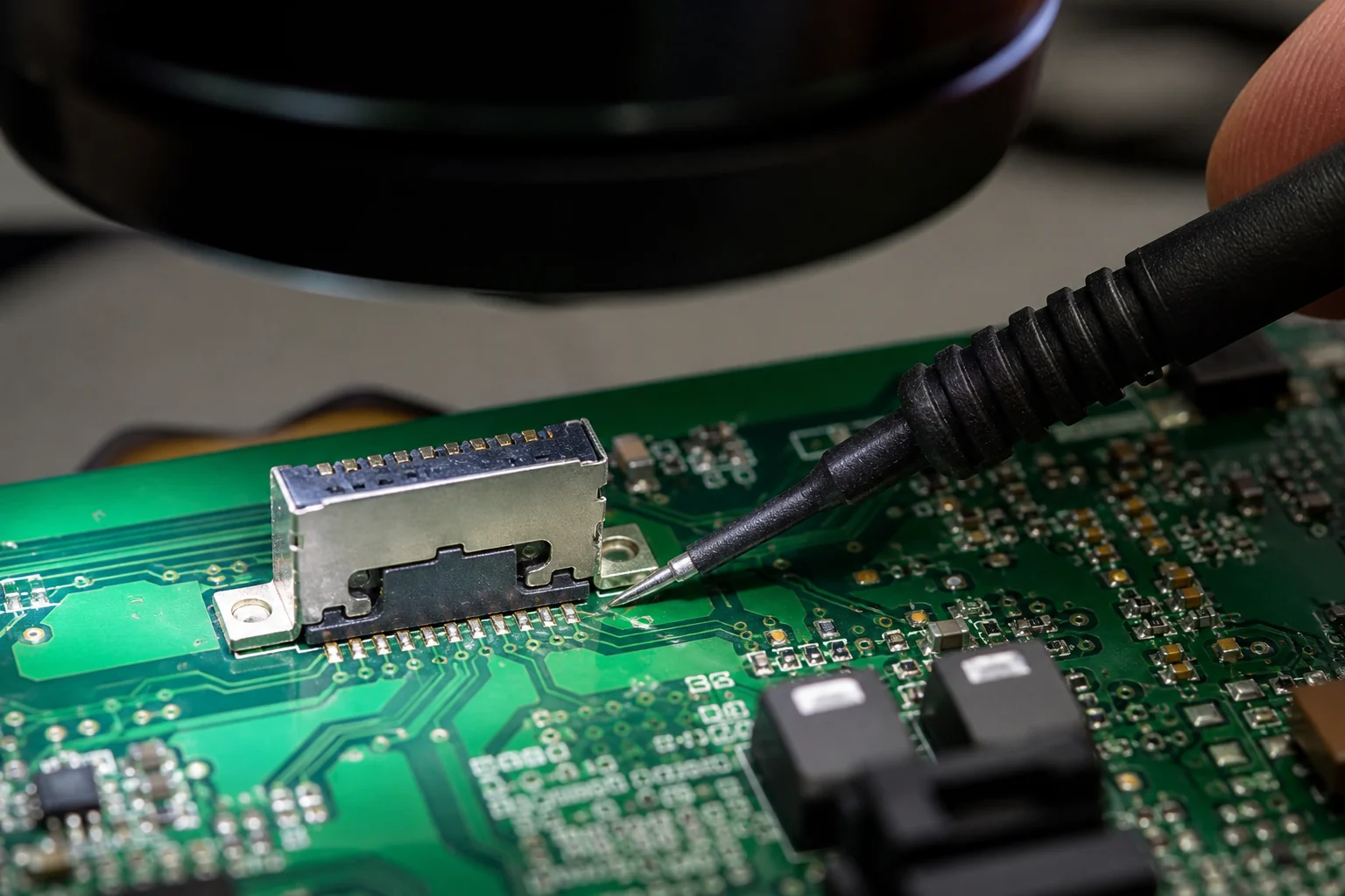
On production boards, the same few structures cause trouble repeatedly. Connector launches are common because the signal sees pad expansion, anti-pad decisions, and sometimes a reference-plane interruption at the exact point where clean energy transfer matters most. Vias are another frequent source because unused barrel length behaves like a stub and shifts the effective structure away from the model.
Return-path breaks are just as dangerous. A trace may look controlled from the top view while its reference plane is split, necked down, or perforated under the route. In that case the mismatch is not only about trace impedance. The return current must detour, loop area grows, and the measured waveform often gets worse than the nominal stackup number would suggest.
- Connector launches with oversized pads or weak anti-pad design.
- Layer transitions that leave long via stubs or poor back-drill decisions.
- Branch stubs on debug headers, test pads, or optional population paths.
- Reference-plane changes that force return current away from the signal path.
- Package escapes where breakout geometry no longer resembles the modeled line.
How to Tell When the Mismatch Is Actually Serious
Not every mismatch deserves a redesign. The severity depends on edge rate, interconnect length relative to rise time, receiver threshold margin, channel loss, and what the interface must pass in production rather than on one friendly bench setup. A short mismatch on a slow control signal may be irrelevant. The same structure on a fast memory, clock, LVDS, RF, or high-speed serial path may become the first reason the board falls out of margin.
Measure the problem in the same context the product will use. If the issue disappears only when the cable is shorter, the fixture changes, or the probe ground is moved, you are already looking at a channel that has little robustness left. That is an engineering warning even if the board can still boot.
What to Check Before You Blame the Calculator
Before recalculating trace width, inspect the real assumptions behind the channel. Confirm the stackup that fabrication actually built, not the one copied from the quote stage. Check whether solder mask thickness, copper roughness, plating, and outer-layer geometry stayed aligned with the impedance model. ReversePCB’s PCB impedance calculator is useful for the baseline line geometry, but it will not rescue a transition that was never modeled properly.
Then examine the discontinuities that the line calculator ignores: launch pads, anti-pads, via stub length, return-path stitching, reference-plane continuity, and any test or assembly branch left attached to the net. If the mismatch originates there, changing the straight-trace width may move the number on a spreadsheet without fixing the real waveform.
How Engineers Usually Measure Impedance Mismatch
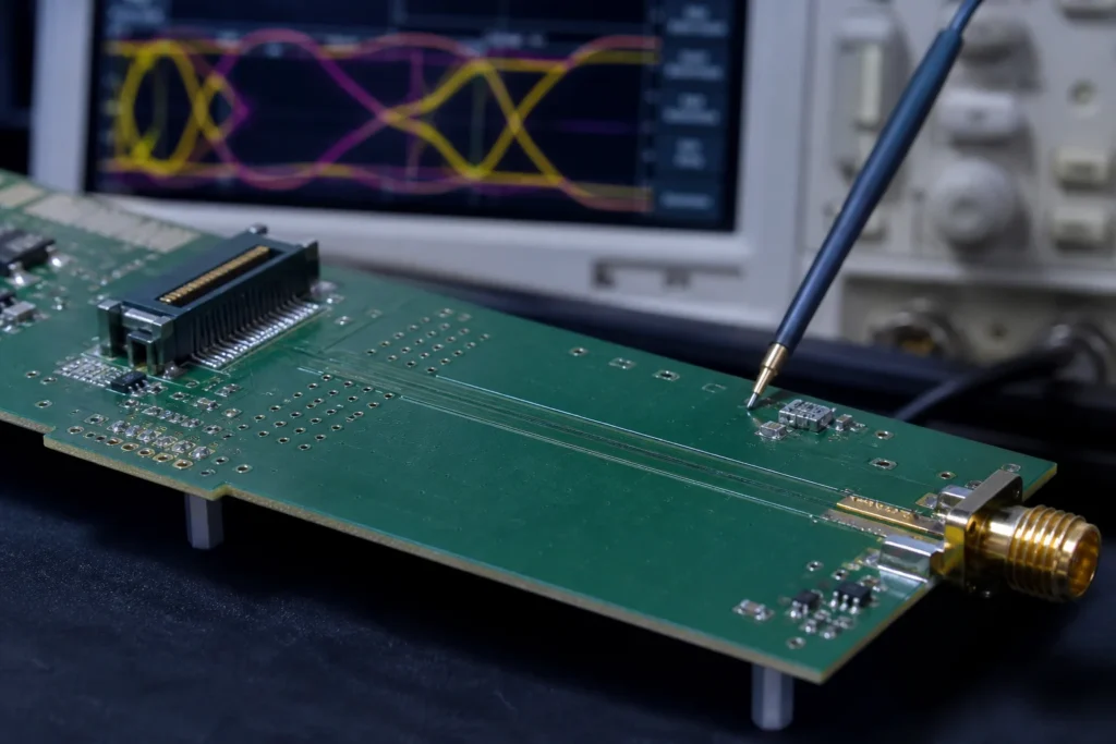
TDR is the clearest method when available because it shows where the channel changes. A VNA helps when the design lives in RF or when insertion and return loss need to be characterized over frequency. High-bandwidth oscilloscope measurements can still be useful for digital channels if you understand the probe loading and the fixture limitations. In all three cases, poor measurement setup can hide or exaggerate the mismatch.
That is why the debug plan matters. If there is no clean way to probe the launch, no coupon that resembles the real structure, or no way to isolate connector and via effects from the rest of the board, the mismatch diagnosis gets slower and more expensive. DFT and SI planning intersect here more than teams often admit.
Fixes That Usually Work Better Than Widening the Trace
Good fixes depend on the discontinuity. Shortening via stubs or back-drilling often helps more than nudging width. A cleaner connector launch can outperform another round of trace tweaking. Adding return-path stitching vias at a plane transition may reduce the effective mismatch because the field sees a more coherent structure. Removing an unnecessary branch stub on a header or test pad can improve the channel immediately.
Termination strategy also matters, especially on digital channels with obvious reflections. The existing ReversePCB article on electronic termination in high speed digital signals is useful once the interconnect geometry is no longer the only issue. But termination should not become an excuse to keep a visibly poor transition if the layout still has room to be corrected.
Why Manufacturing and Assembly Still Matter
Some impedance mismatch problems are born in layout and amplified in fabrication. Drill wander changes anti-pad centering. Plating shifts finished hole geometry. Solder mask on outer layers changes the field environment. Connector coplanarity and assembly tilt can make a launch behave differently from the ideal footprint review. A board that was marginal in the model becomes unstable once process variation pushes it further.
That is also why stackup defaults deserve scrutiny. If you need a reminder that “standard” stackups stop being standard once EMI, cost, and yield start pulling in different directions, the ReversePCB article on standard PCB stackup defaults and tradeoffs complements this topic well.
A Short Review Checklist for PCB Impedance Mismatch
- Confirm whether the mismatch is on the straight line or at a transition.
- Check connector launch pads, anti-pads, and reference continuity before resizing traces.
- Review via stub length, layer changes, and branch stubs on test or debug features.
- Verify the fabricated stackup still matches the modeled impedance assumptions.
- Measure in a setup that reflects the real cable, connector, and fixture environment.
Impedance mismatch becomes easier to solve when you stop treating it as an abstract line-calculation problem. On most boards, it is a geometry transition, return-path, or manufacturability problem wearing a signal-integrity label. Once you identify that real discontinuity, the fix usually becomes much more obvious.
FAQ
Does impedance mismatch always mean the trace width is wrong?
No. Many PCB impedance mismatch problems start at connector launches, via stubs, layer transitions, or return-path breaks rather than on a long uniform trace.
What is the first place to inspect on a mismatch-sensitive PCB channel?
Start with the transition points: connector pads, anti-pads, vias, branch stubs, and any place the reference plane or return path changes.
Can termination fix every impedance mismatch problem?
Termination can reduce reflections in many channels, but it does not replace a poor launch, long via stub, or broken return path. Geometry still matters.
Why can a board pass simulation and still show impedance mismatch in the lab?
Because fabrication build, solder mask, connector behavior, via geometry, and measurement setup can differ from the assumptions used in the original model.