PCB schematics are the backbone of electronics design, serving as a detailed blueprint for how a circuit is constructed on a printed circuit board (PCB). Decoding these schematics is a critical skill for engineers, hobbyists, and anyone working with electronics. Whether you’re designing a new circuit, troubleshooting a malfunctioning board, or simply understanding how a complex system works, being able to read and interpret PCB schematics is essential. This article will guide you through the process of decoding PCB schematics, breaking down their components and helping you understand how to navigate them effectively.
Getting Started with PCB Schematics
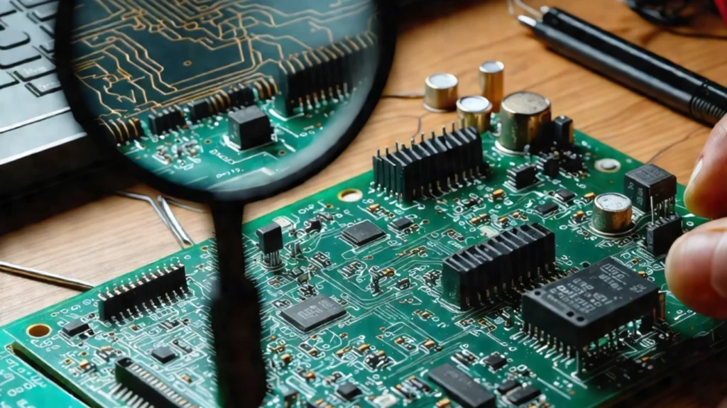
Before diving into the complexities of decoding PCB schematics, you need to gather the right tools and preparation. A magnifying glass is often necessary to read small text and symbols, while a flashlight can help illuminate hard-to-read areas on the board. Familiarize yourself with schematic capture tools like KiCad, Gerber viewers, or Altium, as these will often be your primary tools. Additionally, make sure you have access to component datasheets and manufacturer specifications, as these will be invaluable when interpreting the diagrams.
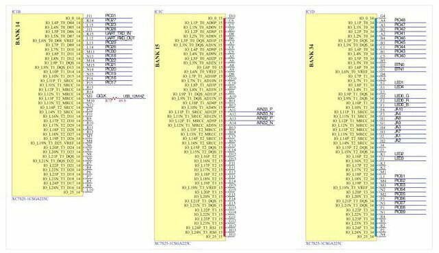
Start by examining the overall layout of the schematic. Look for the netlist, which typically lists all the components and their placements. This can help you identify which parts are present and where they are located on the board. Use the search-and-filter feature of your software to isolate specific components or traces. Begin with the highest-level components and work your way down to the subtle details, keeping track of connections and relationships as you go.
Understanding PCB Layout Components
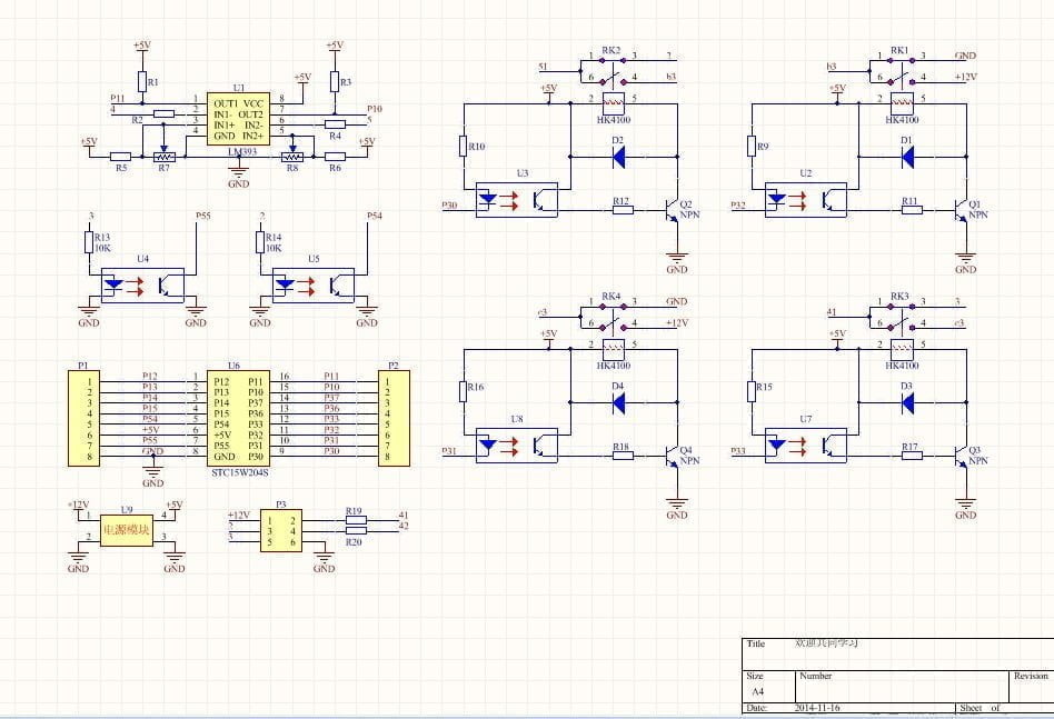
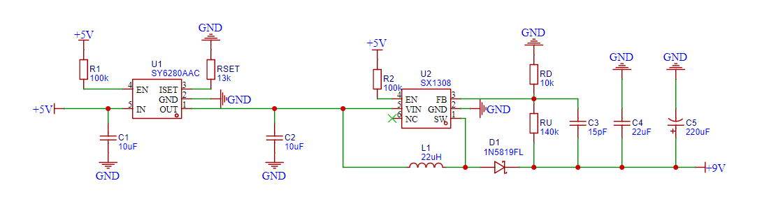
PCB layouts are composed of various elements that work together to create a functioning circuit. The most critical component is the trace, which acts as the path for signals, power, and ground. Traces come in different flavors, such as power traces, ground traces, and signal traces, each with its own color and width. Power and ground traces are usually thicker to handle higher current loads, while signal traces are thinner and designed to minimize signal degradation.
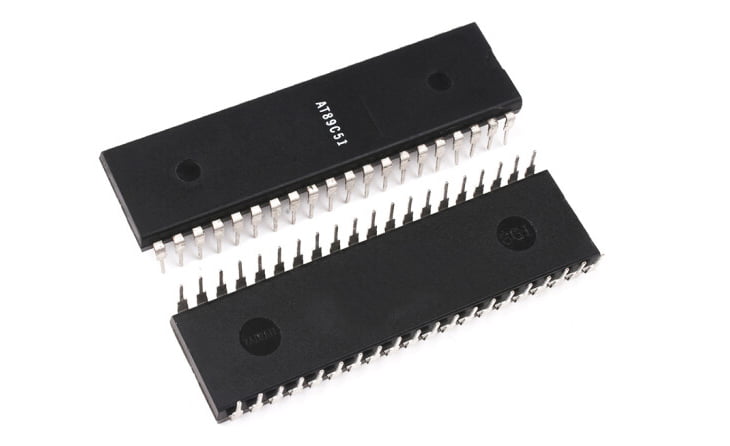
Other key components on the PCB include resistors, capacitors, inductors, voltage regulators, and transistors. Each of these plays a specific role in the circuit’s operation, and their symbols are essential for understanding their function. For example, a triangle with a wavy line represents a capacitor, while a rectangle with two vertical lines indicates a resistor. Pay attention to how these components are interconnected and how they contribute to the overall circuit design.
Decoding Trace Routes and Signals
One of the most challenging aspects of decoding PCB schematics is tracing the route of a signal from one component to another. Signals are represented by lines (traces) connecting components like microcontrollers, memory, and peripherals. The goal is to follow these traces to understand how the circuit operates and identify potential issues. Look for arrows and direction indicators (such as small circles or squares) that show the flow of current and data.
Be on the lookout for critical points where signals enter or leave a component, such as inductors, decoupling capacitors, or voltage regulators. These elements can create voltage drops, noise, or bottlenecks that affect the circuit’s performance. By examining these traces, you can gain insights into how the circuit is designed to handle power, ground, and signal integrity.
Analyzing Power and Ground Distribution
Power and ground distribution is another critical aspect of PCB schematics. These traces must supply sufficient current to all components without causing voltage drops or overheatting. Look for large power traces that feed into voltage regulators or power management circuits, as these are often the first points of failure. Ground traces, on the other hand, must provide a stable reference for the circuit and minimize noise interference.
In high-speed circuits, you may encounter grounding techniques like the ground plane and bypass capacitors. These are designed to suppress noise and ensure stability. By analyzing the distribution of power and ground traces, you can identify potential red flags, such as traces that are too thin for the current they carry or wiring that is too long, leading to inductive resistance.
Reading Schematic Symbols and Legends
Schematic symbols and legends are the visual keys to understanding the circuit’s design. Each symbol represents a specific component and its electrical properties. For example, an open rectangle with two vertical lines indicates a resistor, while a circle with a cross inside represents a capacitor. The legend, which is a list of symbols and their corresponding components, is essential for decoding the schematic accurately.
Take the time to familiarize yourself with common symbols and their meanings. For instance, a triangle with a vertical line in the middle is a diode, while a square with a curved line at the top is an inductor. Use the legend as a reference while examining the schematic, and you’ll be able to decode even the most complex diagrams.
Putting It All Together
Decoding PCB schematics is a complex process that requires patience, practice, and a good understanding of electronics fundamentals. Start by focusing on one section of the schematic at a time, and gradually build your expertise. Use the tools and resources available to you, such as simulation software and online forums, to assist with troubleshooting.
By analyzing the layout, traces, power distribution, and component symbols, you’ll gain a deeper understanding of how the circuit operates. This knowledge will not only help you design better circuits but also enable you to troubleshoot and optimize existing ones. So, dive into the world of PCBs and let your curiosity guide you as you unlock the secrets of circuit design.
Decoding PCB schematics is a rewarding process that offers insights into the inner workings of electronic circuits. With the right tools, a systematic approach, and a willingness to learn, anyone can master this skill. Whether you’re a seasoned engineer or a hobbyist, understanding PCB schematics will empower you to design, simulate, and test circuits with confidence. So, grab a magnifying glass, fire up your software, and let’s get decoding!