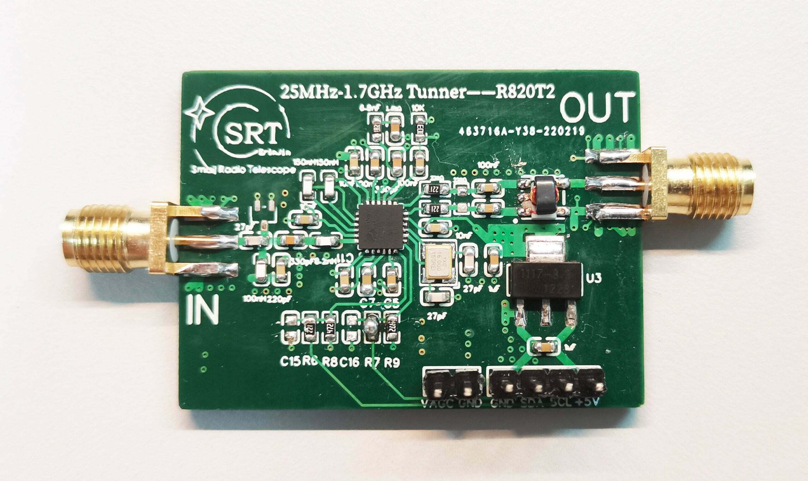
What Are High-Frequency PCBs?
Key Features of High-Frequency PCBs in Communication Circuits
Signal Integrity
Signal integrity plays a key role in high-frequency communication circuits. Problems like signal reflection, attenuation, and delay can hurt performance. To tackle these issues, designers need to use impedance matching differential signaling, and careful ground/power line routing.
Specialized Materials
High-frequency PCBs in communication circuits use materials with low dielectric constants and low signal loss. Examples include PTFE (polytetrafluoroethylene) and Rogers laminates. These materials help to minimize signal degradation and allow signals to move faster.
Layer Stack-up Design
Communication circuits require an optimized PCB stack-up. This is vital to cut down on interference and crosstalk, which ensures clear and reliable signal transmission.
Design Principles for High-Frequency PCB
To create high-frequency PCBs for communication circuits, engineers need to keep these key points in mind:
Impedance Matching:
Good impedance matching plays a key role to ensure reliable signal transmission in communication systems. Signals at high frequencies react more to changes in impedance, and when things don’t match up, it can lead to signal bouncing back or getting weaker.
Differential Signal Transmission:
Using differential signaling helps to cut down on common-mode noise, which in turn reduces electromagnetic interference (EMI) in communication circuits. Many people use this method to boost signal reliability.
Power and Ground Plane Layout:
Big well-organized power and ground planes help to keep interference and noise low, which is crucial for communication circuits that need to perform well at high speeds.
Via Design:
Keeping the number of vias low and using blind or buried vias can make signal integrity better by cutting down on unwanted effects. This matters a lot in multilayer PCBs that communication circuits use.
Manufacturing Techniques for High-Frequency PCBs
Companies need to be precise when they make high-frequency PCBs for communication circuits:
Lamination and Copper Plating:
Laminating multiple layers and plating copper helps ensure that all layers of the PCB connect.
Surface Treatment:
Methods like immersion gold or tin spraying help protect the PCB surface and make it easier to solder.
Testing:
Thorough testing of electrical performance is crucial to meet the strict needs of communication systems.
Future Trends in High-Frequency PCB Communication Circuits
As communication circuits become more complex and demand better performance several trends are changing the future of high-frequency PCBs:
Advanced Materials:
Scientists will create new materials that have lower dielectric constants and loss factors. These materials will meet the changing needs of communication circuits.
Better Manufacturing Processes:
High-precision manufacturing will keep getting better. It will use more complex layer stack-ups and cut down on signal interference.
Better Design Tools:
Professional design software like Altium Designer and Cadence will become smarter. This will help designers make high-frequency communication circuits more quickly.
Smart Manufacturing:
Automation and AI will have a bigger role in making PCBs. This will ensure that communication circuit boards are more accurate and have fewer flaws.
Conclusion
High-frequency PCBs play a key role in modern communication circuits. They help signals move faster and more . As tech gets better so will the ways we design and make these PCBs. This means they’ll stay crucial to how communication systems work. In the future, we’ll see PCBs that work even better and do more. These new PCBs will push forward new ideas in phone networks and other fields.


