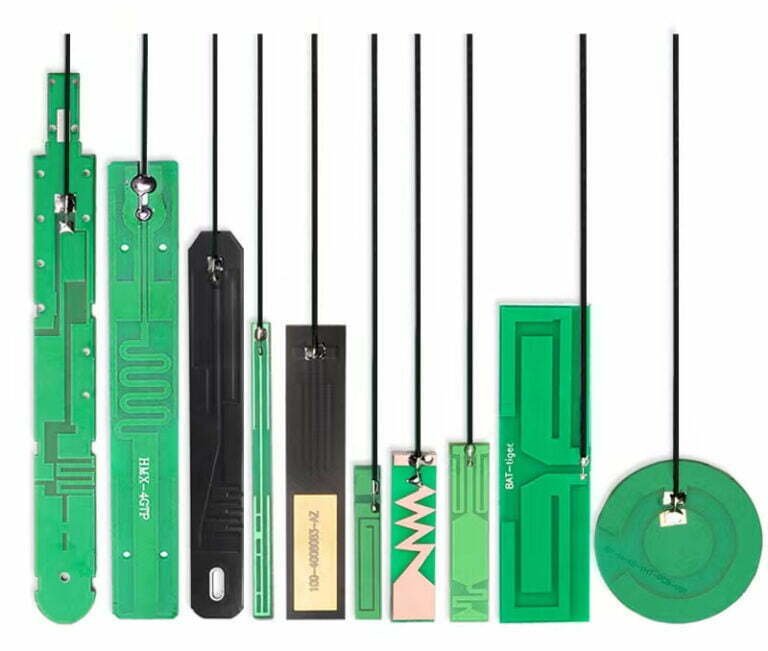
PCB antennas are an integral part of many modern electronic devices. They enable wireless communication, allow for remote control of devices, and provide a means for transmitting data to and from the device. With the right design and implementation, PCB antennas can significantly improve the performance of any device. In this blog article, we will discuss the basics of PCB antenna technology, the advantages of PCB antennas, common types of PCB antennas, design considerations, common applications, testing and measurement, and tips for improving performance.
Introduction to PCB Antenna Technology
A PCB antenna is a small antenna that is integrated onto a printed circuit board. They are typically used for short-range radio communication and data transmission. PCB antennas can be used in a variety of applications, such as Bluetooth and Wi-Fi devices, UAVs, and radio-frequency identification (RFID) systems. PCB antennas come in a variety of shapes and sizes and can be made from different materials. The most common type of PCB antenna is the dipole antenna, which consists of two metal rods arranged in an “X” shape.
The design of PCB antennas is based on the principles of electromagnetic radiation. Electromagnetic radiation is generated when electric and magnetic fields interact with each other. When an antenna is placed in an electric field, it will generate a signal, which can be transmitted or received. The antenna can also be used to receive signals from other sources, such as satellites or ground stations. The type of antenna and its design will determine the characteristics of the signal it can generate and receive.
PCB antennas are used in a variety of applications, such as wireless communication and remote control. They are an essential component of many modern devices, such as smartphones, tablets, and laptops. They are also used in consumer electronics, such as televisions, audio systems, and gaming consoles.
Advantages of PCB Antennas
PCB antennas offer several advantages over traditional antennas. They are relatively inexpensive, easy to manufacture, and can be integrated into a variety of devices. The small size of PCB antennas also makes them ideal for use in portable applications, such as mobile phones and tablets.
PCB antennas are also more reliable than traditional antennas. They are less prone to mechanical damage, and their performance is less affected by environmental factors, such as wind and rain. PCB antennas also offer a higher degree of flexibility, as they can be designed to meet specific requirements.
Another advantage of PCB antennas is that they are relatively easy to install. They can be mounted directly onto the circuit board and require only a few simple connections. This makes them ideal for applications where space and weight are at a premium.
Common Types of PCB Antennas
There are a number of different types of PCB antennas, each of which has its own advantages and disadvantages. The most common types are dipole, monopole, and patch antennas.
dipole antenna
The dipole antenna is the most common type of PCB antenna. It consists of two metal rods arranged in an “X” shape. The dipole antenna is a balanced antenna, meaning that both rods have the same electrical length. The dipole antenna is typically used for short-range applications, such as wireless communication and remote control.
monopole antenna
The monopole antenna is another common type of PCB antenna. It consists of a single metal rod and is typically used for medium-range applications, such as GPS and cellular communication.
patch antenna
The patch antenna is a type of antenna that consists of a metal patch on a substrate. It is typically used for long-range applications, such as satellite communications. Patch antennas are typically more efficient than dipole and monopole antennas, but they are more difficult to design and manufacture.
PCB Antenna Design Considerations
The design of a PCB antenna requires a number of factors to be taken into consideration, such as the size of the antenna, the dielectric constant of the PCB material, the amount of copper used, and the surrounding environment.
type of antenna
The first is the type of antenna. As mentioned above, there are a number of different types of antennas, each of which has its own advantages and disadvantages. The type of antenna should be chosen based on the application and the desired performance.
antenna’s frequency range
The second consideration is the antenna’s frequency range. The frequency range is the range of frequencies that the antenna can transmit and receive. The frequency range should be chosen based on the application and the desired performance.
antenna’s gain
The third consideration is the antenna’s gain. The gain is a measure of the antenna’s power and is typically expressed in decibels (dB). The gain should be chosen based on the application and the desired performance.
antenna’s radiation pattern
The fourth consideration is the antenna’s radiation pattern. The radiation pattern is a measure of the antenna’s ability to transmit and receive signals in different directions. The radiation pattern should be chosen based on the application and the desired performance.
antenna’s size and shape
Finally, the antenna’s size and shape should be considered. The size and shape of the antenna will affect its performance, so it needs to be chosen carefully.
PCB antenna formula calculating
The design of a PCB antenna requires a number of factors to be taken into consideration, such as the size of the antenna, the dielectric constant of the PCB material, the amount of copper used, and the surrounding environment.
PCB Antenna Gain
The formula for the PCB antenna gain is given by the following equation:
Antenna Gain (dB) = 10*log(4*pi*d^2/λ^2)
where d is the effective length of the antenna, and λ is the wavelength of the signal. This equation is often used to calculate the gain of a PCB antenna in decibels (dB).
The gain of a PCB antenna is determined by the size of the antenna, its shape, and the materials used. Generally speaking, the larger the antenna, the higher the gain. Also, certain materials, such as copper, can increase the gain of a PCB antenna due to their higher conductivity. The shape and orientation of the antenna also affect the gain, with more complex shapes and orientations providing a higher gain.
In addition to the formula above, there are other methods for determining the gain of a PCB antenna, such as using simulations or measurements of the actual antenna. These methods are more accurate than the formula, but can be more time consuming.
PCB Antenna length
The another important factor when designing a PCB antenna is the size and shape, which can affects the maximum efficiency. The equation is as follows:
Antenna length = (λ/2π) x √[(εr + 1)/2]
Where λ is the wavelength of the signal, εr is the dielectric constant of the PCB material, and 2π is a constant. The antenna length is given in meters.
Once the antenna length is calculated, the shape of the antenna can be determined. Commonly used shapes are a dipole, monopole, or loop antenna. The choice of the shape will depend on the application and the desired performance. Care must also be taken to ensure that the antenna is correctly tuned to the desired frequency.
By using above antenna formula, it is possible to accurately design a PCB antenna that is both cost-effective and reliable.
Friis Transmission Equation
The most commonly used formula for designing a Printed Circuit Board (PCB) antenna is the Friis Transmission Equation, which describes the power received by an antenna in terms of the transmitted power and the distance between the transmitting and receiving antennas. The equation takes into account various factors such as the gain of the transmitting antenna, the gain of the receiving antenna, the wavelength of the signal, and the distance between the two antennas. The equation can be expressed as:
Pt = Pr + Gt + Gr – 20 log (d) – 20 log (λ)
Where Pt is the transmitted power, Pr is the power received, Gt is the transmit antenna gain, Gr is the receive antenna gain, d is the distance between the two antennas, and λ is the wavelength of the signal. This equation can be used to calculate the power received at any given distance between the two antennas. It is important to note that the gains of both antennas must be known in order to use this equation effectively.
Common Applications for PCB Antennas
PCB antennas are used in a variety of applications, such as wireless communication, remote control, and data transmission. They are commonly used in consumer electronics, such as smartphones, tablets, and laptops. They are also used in other applications, such as radio-frequency identification (RFID) systems, automotive systems, and UAVs.
PCB antennas are also used in satellite communication systems, such as GPS and GLONASS. They are also used in medical devices, such as pacemakers and hearing aids.
PCB Antenna Testing and Measurement
When designing a PCB antenna, it is important to test and measure its performance. This can be done using a variety of methods, such as return loss measurements, gain measurements, and radiation pattern measurements.
Return loss measurements
Return loss measurements measure the amount of power reflected back to the antenna. This information can be used to determine the antenna’s efficiency and to determine any issues with the antenna design.
Gain measurements
Gain measurements measure the amount of power transmitted by the antenna. This information can be used to determine the antenna’s range and power output.
Radiation pattern measurements
Radiation pattern measurements measure the antenna’s ability to transmit and receive signals in different directions. This information can be used to determine the antenna’s coverage area and to identify any potential issues with the antenna’s design.
Tips for Improving PCB Antenna Performance
There are a number of steps that can be taken to improve the performance of a PCB antenna. These include:
- Optimizing the antenna’s design. This can be done by changing the antenna’s size and shape, as well as by changing the materials used.
- Minimizing the antenna’s losses. This can be done by reducing the amount of attenuation in the antenna’s feed line, as well as by reducing the amount of interference from other components.
- Minimizing the antenna’s gain. This can be done by reducing the antenna’s size and shape and by optimizing the antenna’s design.
- Optimizing the antenna’s radiation pattern. This can be done by changing the antenna’s size and shape, as well as by changing the materials used.
- Improving the antenna’s performance in different environments. This can be done by testing the antenna in different environments and by making adjustments to the antenna’s design accordingly.


