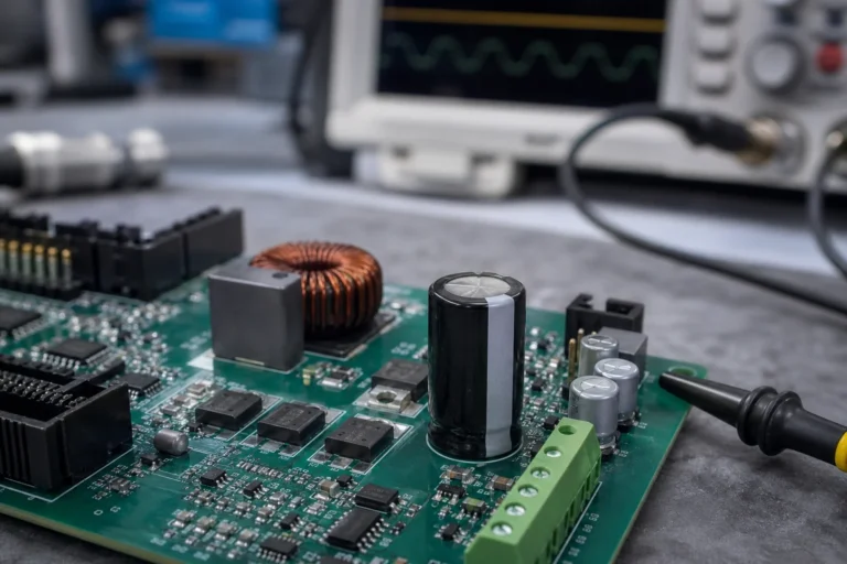
How to Choose an Electrolytic Capacitor for a PCB Power Stage
Learn how to choose an electrolytic capacitor for PCB power stages by checking ripple current, ESR, temperature, package layout, and the failure modes that cause repeat board repairs.

Learn how to choose an electrolytic capacitor for PCB power stages by checking ripple current, ESR, temperature, package layout, and the failure modes that cause repeat board repairs.
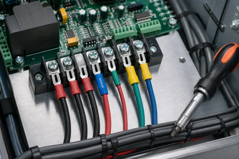
A spade connector is useful when electronics wiring needs quick service access, but it becomes a liability if vibration, poor crimp control, or hidden screw joints can let the fork walk loose.
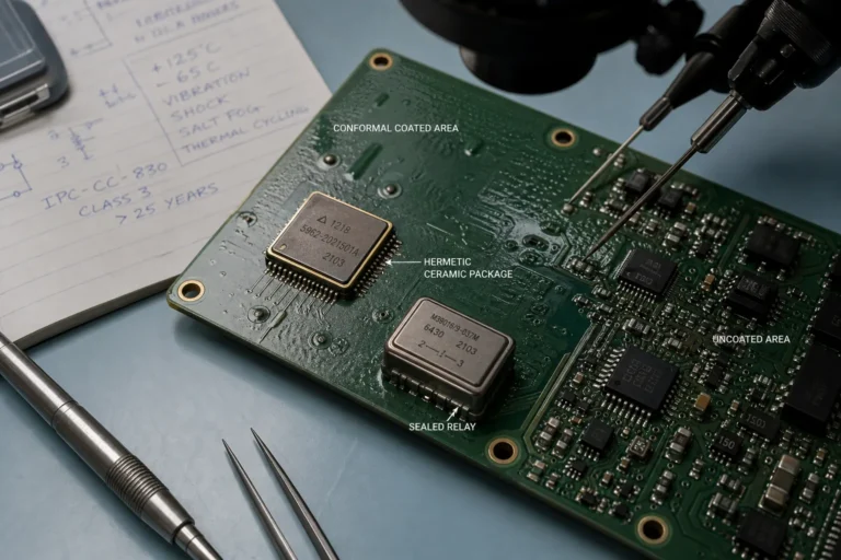
Hermetically sealed components earn their cost only when moisture, outgassing, pressure cycling, or long service intervals make ordinary coating and enclosure strategies unreliable.
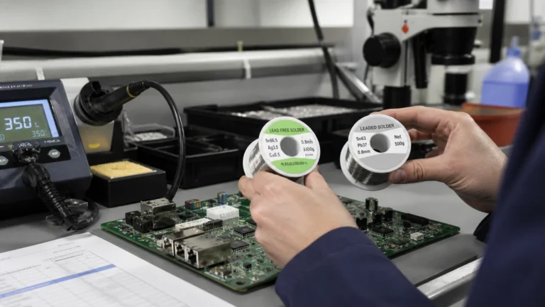
Lead versus lead-free solder changes reflow margin, repair behavior, compliance, and hole-fill control, so the right choice depends on the full PCB assembly lifecycle.
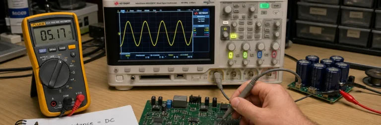
Resistance explains static loss and voltage drop, but impedance decides how PCB traces, capacitors, drivers, and interconnects behave once frequency and edge rate matter.
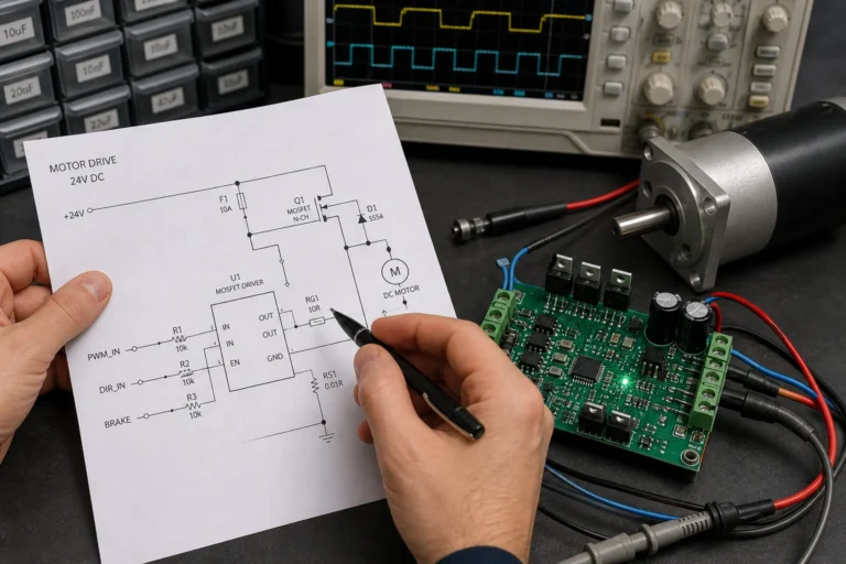
A motor schematic symbol only becomes useful when you read it with the power path, control method, and protection details that surround the load.
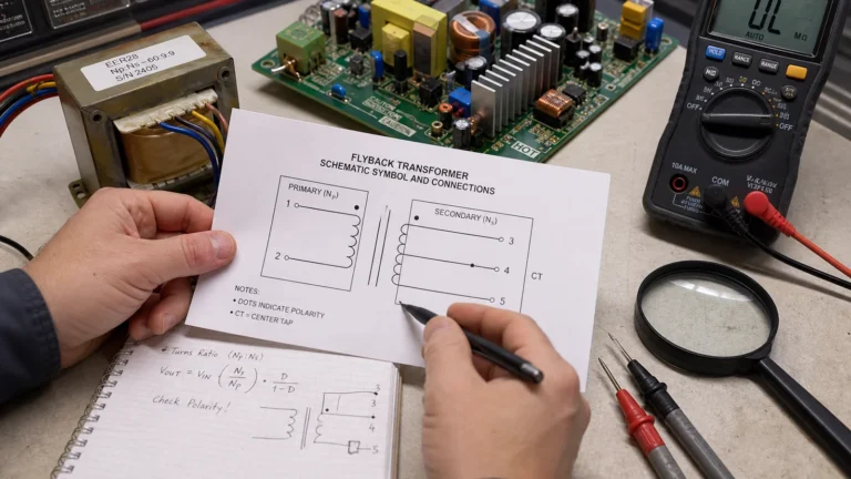
A transformer schematic symbol only helps when it makes winding polarity, taps, isolation, and real circuit intent clear enough for layout, test, and repair work.
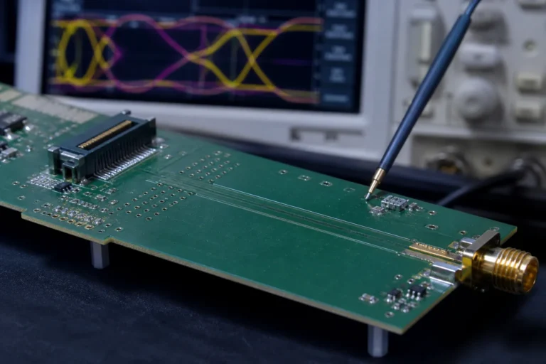
Impedance mismatch on a PCB usually appears first at the launch, via field, connector, or return-path break where the signal stops seeing the geometry you modeled.
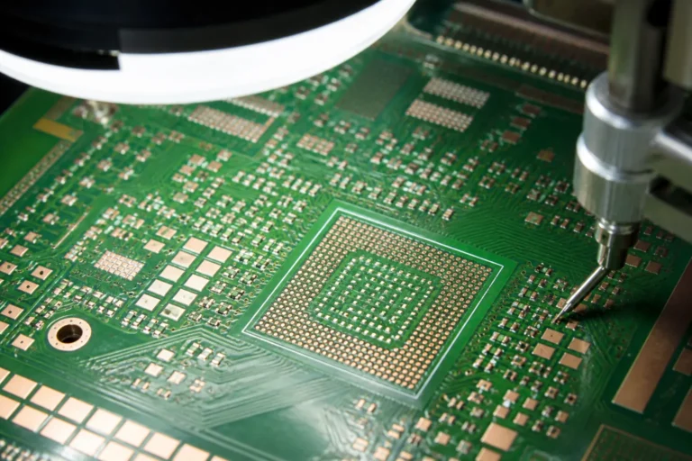
PCB solder mask thickness matters when it starts changing pad definition, inspection clarity, outer-layer impedance assumptions, and the assembly window around dense features.
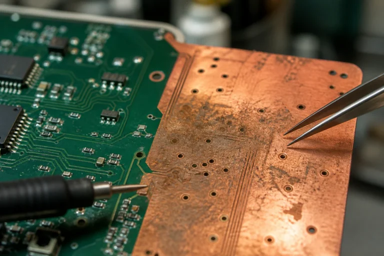
A PCB without solder mask can oxidize, stain, bridge during assembly, and become harder to inspect or rework unless the exposed copper area is intentional and tightly controlled.