Hermetically sealed parts usually enter a PCB discussion after a standard protection stack has already started to look weak. The board may live in condensation, aggressive vapors, long storage intervals, pressure cycling, or a service environment where one latent moisture failure costs more than the package premium ever would. In those cases, the right question is not whether hermetic packaging sounds robust. It is whether the failure you are trying to prevent actually passes through the package boundary.
This guide focuses on that decision from a board-level perspective: when hermetically sealed components are the right move, what they still do not protect, and where conformal coating, potting, sealed connectors, or a better enclosure solve the problem more efficiently.
What hermetically sealed means in electronic packaging
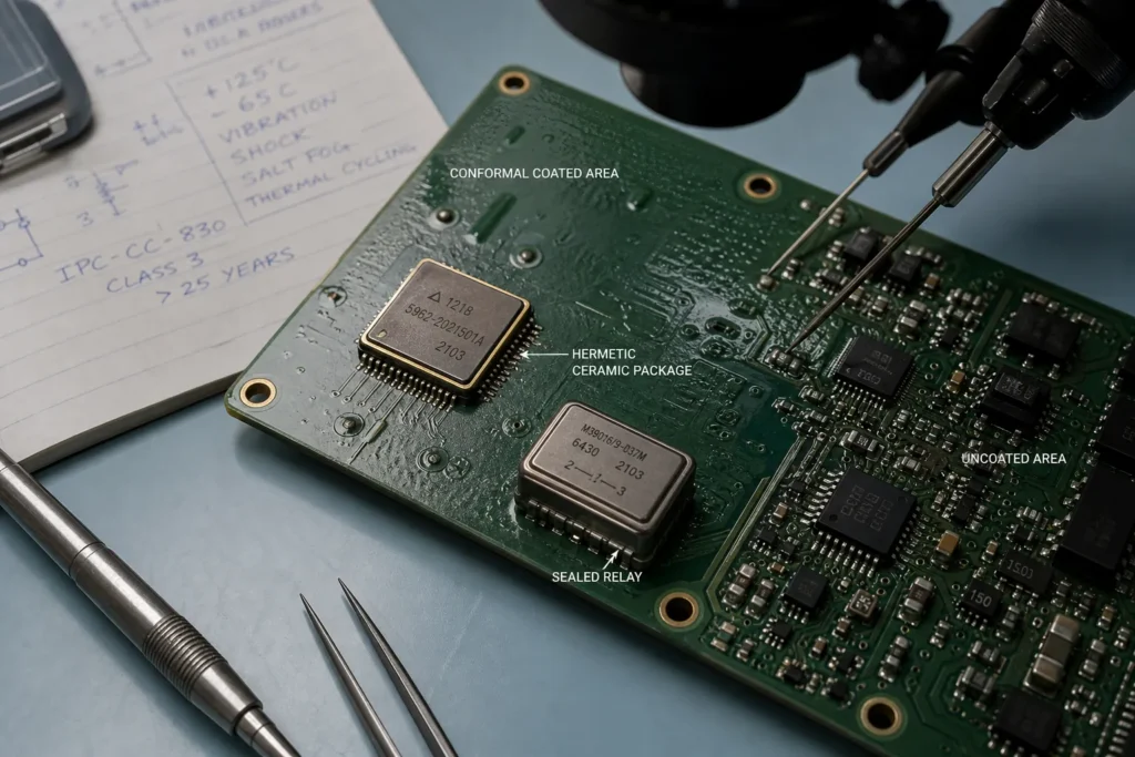
In electronics, hermetically sealed normally means the package is built to keep gases and moisture from moving through the seal path at a tightly controlled leak rate. That is a different claim from being splash-resistant, conformal-coated, gasketed, or simply enclosed in plastic. Hermetic packages are common in ceramic, glass-to-metal, and metal-can constructions where the die, cavity, or sensitive internal structure cannot tolerate ordinary environmental ingress over the intended life.
For PCB teams, that distinction matters because the package may be hermetic while the assembly around it is not. A sealed sensor, relay, crystal, or hybrid module can remain stable internally, but the solder joints, connector interfaces, exposed copper, test pads, and contamination trapped under nearby components can still become the dominant failure points.
When a hermetic package is worth the cost
Hermetic parts usually earn their keep when the board must survive an environment that keeps attacking the inside of ordinary packages faster than the rest of the system can compensate. That often shows up in aerospace, defense, downhole, industrial process control, medical implants, high-reliability sensing, and long-idle equipment that has to wake up years later without guessing whether moisture drifted into the component body.
Three triggers make the cost easier to justify:
- The component itself is the weak environmental boundary. Crystals, MEMS sensors, relays, RF modules, and certain hybrids can shift or fail because of internal moisture, contamination, or gas interaction rather than because of board-surface corrosion alone.
- The inspection and repair model is expensive. If replacing one failed module means field disassembly, recalibration, recertification, or loss of mission time, the package premium may be cheaper than one avoidable return.
- The environment keeps defeating softer protections. If coating chemistry, vent paths, wash residue, or enclosure breathing already caused trouble in earlier builds, moving the barrier to the component package can be the cleaner fix.
Where engineers over-specify hermetic components
A hermetic package is not a substitute for system design discipline. Teams often over-buy it when the real failure path sits outside the component. If condensation bridges high-impedance nodes on the PCB, if flux residue keeps leaking current after coating, or if the connector side is taking repeated surge and contamination stress, a hermetic IC package will not solve the dominant problem. In that case the better spend may be board cleaning, spacing, enclosure airflow control, a sealed connector, or stronger interface protection such as the TVS suppressor diode guide covers for I/O survival.
This is also where procurement pressure distorts decisions. A buyer may see the hermetic option as a reliability upgrade in every harsh-environment design, while manufacturing sees longer lead time and test complexity, and service sees harder replacement choices. If the package is protecting a part that would already survive with good enclosure and board protection, the extra cost can quietly land in BOM without improving the actual return rate.
The board-level risks hermetic sealing does not remove
Even the best hermetically sealed component leaves several board-level risks untouched.
- Solder-joint fatigue and CTE mismatch. Ceramic and metal packages can be less forgiving than plastic packages during thermal cycling. The cavity may stay dry while the solder fillet cracks.
- Assembly-process stress. Heavier packages, stiffer leads, and different thermal mass can change reflow behavior, voiding patterns, and pad design choices.
- Under-component contamination. If cleaning is weak, ionic residue beneath neighboring parts can still drive leakage or dendritic growth. The post-solder cleaning guide is more relevant here than a better package seal.
- Connector and harness ingress. Many harsh-environment failures begin at cable entries, feedthroughs, and unsealed mating interfaces, not inside the active component body.
- Test and service access. Potting, shielding cans, or sealed subassemblies added around a hermetic part can make diagnostic access worse if the test strategy is not planned early.
That is why hermetic-package selection should sit inside a wider DFM and DFT review. If the team cannot inspect the solder joints, verify leak-sensitive calibration after assembly, or replace the part without collateral damage, the reliability story is incomplete.
How to choose between hermetic parts, coating, potting, and sealed connectors
The most practical decision framework is to ask where the barrier needs to sit.
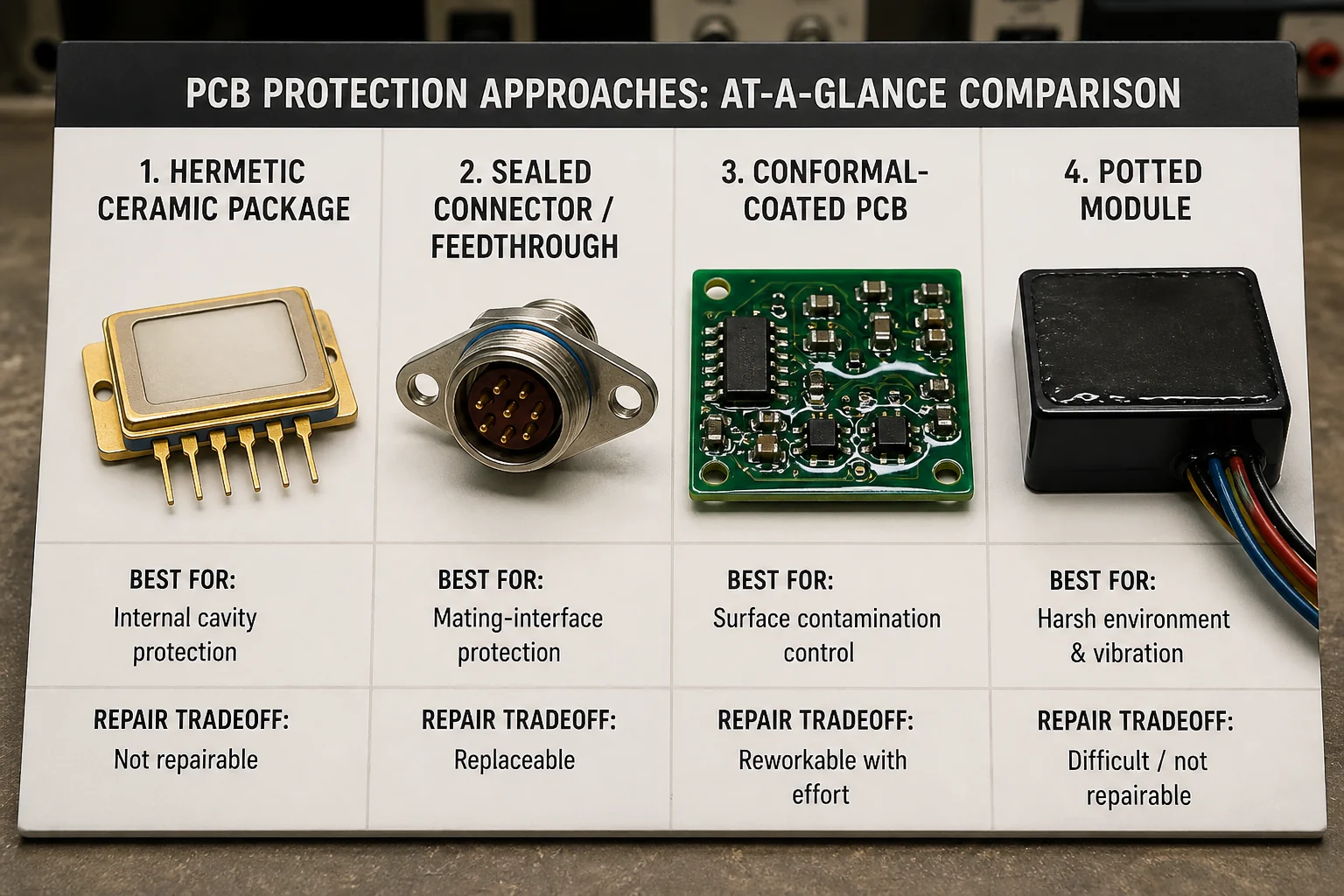
If the component cavity must stay chemically stable, hermetic packaging is the right layer. If the whole board only needs moisture and residue resistance, a validated PCB conformal coating guide approach is often cheaper and more repairable. If the field failures come from cable-side ingress, sealed connectors and strain relief matter more. If tamper resistance, vibration, and environmental isolation all matter together, potting may be the stronger answer, but it raises rework and heat-dissipation penalties immediately.
Put differently: hermetic packages protect the inside of the part, coating protects exposed board surfaces, sealed connectors protect the mating interface, and potting protects the assembly by sacrificing easy repair. Mixing those roles up is a common specification mistake.
Package and layout details that deserve extra attention
Once a hermetic part is selected, layout and assembly details become less forgiving. Ceramic leadless packages, metal cans, and glass-to-metal feedthrough parts can impose tougher footprint, coplanarity, and thermal-profile demands than an ordinary molded package. Some of the same footprint discipline described in the leadless chip carrier guide becomes relevant again: pad geometry, inspection angle, and how easily hidden joints can be verified after reflow.
It is also worth checking whether the package creates nearby keep-out, wash, or coating constraints. A sealed relay or sensor may survive solvent exposure internally, yet the manufacturer can still limit ultrasonic cleaning, side loading, or mechanical shock during depanelization. These are exactly the details that disappear when the team treats hermetic packaging as a simple premium checkbox.
Inspection checkpoints before you sign off the design
Before release, a useful review asks for evidence instead of adjectives.
- What failure mode is the hermetic package blocking? Moisture drift, corrosion, gas contamination, calibration shift, internal contact degradation, or something else.
- Is the package leak performance actually specified and verified? High-reliability programs may require formal leak-test evidence rather than vendor marketing language.
- What happens at the solder joint during temperature cycling? A dry internal cavity does not protect against board-level strain.
- Can incoming inspection distinguish genuine hermetic parts from visually similar commercial substitutes? This matters in mixed sourcing or broker-risk environments.
- What is the repair reality? If the package is expensive, scarce, or heat-sensitive during removal, service planning needs to be explicit.
Those checkpoints also help buyers and program managers understand why the part is in the BOM. Without them, hermetic selections can survive long after the actual environmental requirement has changed.
When hermetic sealing is the right answer
Hermetically sealed components make sense when the internal cavity of the part is genuinely the reliability bottleneck and the system cannot accept drift, corrosion, or environmental aging there. They do not make sense as a generic substitute for enclosure design, contamination control, connector sealing, or proper board protection. If the environment is attacking the PCB surface, fix the PCB surface. If it is attacking the component internals over years of service, then a hermetic package may be exactly the right line item to defend.
The strongest designs are usually the ones that place each barrier where it belongs instead of asking one expensive package choice to solve every harsh-environment problem at once.
FAQ
What does hermetically sealed mean for an electronic component?
It means the package is built to limit gas and moisture ingress through the seal path to a tightly controlled leak rate, typically using ceramic, metal, or glass-to-metal construction rather than relying on ordinary molded plastic alone.
Are hermetically sealed components always better for harsh-environment PCBs?
No. They help when the component cavity itself is the environmental weak point. If failures come from board residue, connector ingress, surge exposure, or enclosure breathing, coating, sealing, cleaning, or interface protection may be the better fix.
Can a hermetic package still fail on a PCB?
Yes. The internal cavity may stay protected while the solder joints crack, the board corrodes, the connector leaks, or contamination under nearby parts causes electrical leakage. Hermetic packaging does not remove normal board-level reliability work.
How do I choose between hermetic parts and conformal coating?
Choose hermetic packaging when the inside of the component must stay stable over time. Choose conformal coating when the main risk is on exposed board surfaces. Some high-reliability designs use both, but they solve different problems.