An Altium net tie is useful when two nets really do need to meet, but only at one deliberate location that still has to survive review, layout, and manufacturing. The common failure is not forgetting the feature exists. It is using it as a shortcut after the project already has confused ground naming, sloppy return-path planning, or a layout rule problem that should have been fixed at the source.
If the design requirement is real, a net tie can keep two net names separate while allowing one controlled short on the PCB. If the requirement is vague, the same part can hide a routing mess until polygon pours, DRC, test coverage, or a later ECO exposes what the schematic never made clear.
What an Altium Net Tie Actually Does
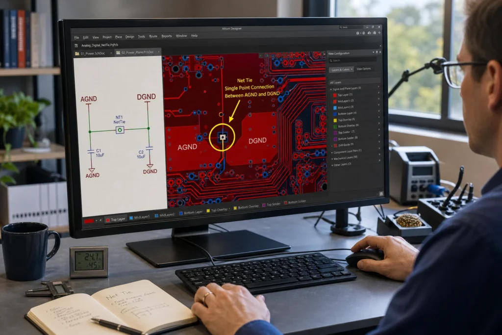
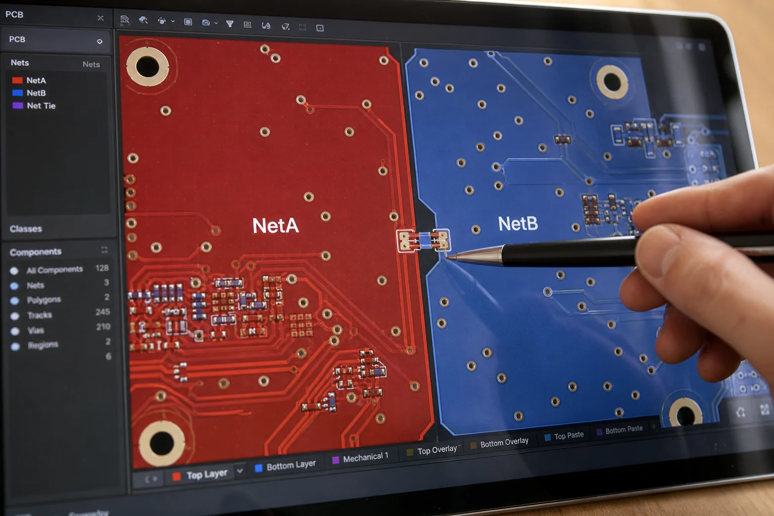
In Altium, a net tie is a controlled short circuit implemented as a component type. The schematic symbol carries separate pins for the nets you want to join, while the PCB footprint contains the copper that physically shorts them together. That matters because the nets do not lose their names across the rest of the design. You keep separate rule scopes, labeling, and review visibility everywhere except at the exact join point.
That behavior is why net ties are useful for cases like AGND to DGND joins, Kelvin sense routing, current-shunt breakouts, or a planned star connection where one short location is intentional and every other short would be a mistake. It is not the right answer when the team has not decided whether the nets should really stay separate.
When a Net Tie Is Better Than a 0-Ohm Resistor
A 0-ohm resistor is the better choice when you may want assembly options, debug removal, or a BOM-visible jumper. A net tie is better when the short is part of the geometry itself and should not become a purchasing line item, placement decision, or accidental substitution later. In other words, if the connection is fundamentally copper, treat it like copper.
This distinction becomes practical during NPI builds. If a technician may need to cut, stuff, or replace the connection to isolate a fault, a resistor or header usually creates less ambiguity. If the join exists only to preserve two net names until one exact footprint location, the extra component often adds clutter without solving anything.
Where Engineers Commonly Use Net Ties
The cleanest use cases are the ones where the join point has design meaning. Mixed-signal boards often separate analog and digital grounds long enough to control current return paths, then connect them at one reviewed point near a converter or shunt path. Power boards sometimes keep noisy current paths named separately from sensitive measurement nets so layout rules, polygon priorities, and design reviews stay readable.
Another strong use case is current sensing. If you want force and sense nodes to remain distinct in the schematic and rules but still meet in a precise copper feature, a net tie prevents the entire design from collapsing into one generic net name. The same logic applies to some RF and planar copper structures where the short is intentional but must remain localized.
What Goes Wrong When a Net Tie Is Used as a Shortcut
The first mistake is hiding unresolved grounding strategy behind a footprint. A net tie does not fix poor partitioning. If AGND and DGND were split without a real return-current reason, reconnecting them later with a net tie only preserves the confusion in a more complicated form.
The second mistake is footprint construction. Altium expects the short to live inside the net tie footprint. If the copper bridge is too small, isolated, or routed incorrectly, you can end up with verification failures or pours that do not connect the way the designer expected. This often shows up late, when someone repours polygons and suddenly the controlled short behaves more like an accidental island.
The third mistake is BOM and assembly confusion. Some joins belong in the BOM, others do not. If the connection might later become a resistor, ferrite bead, or jumper, choose the component style deliberately. Otherwise, procurement and assembly documentation may imply a selectable part where the design really intended a fixed copper join.
How to Build a Net Tie Without Causing DRC Trouble
Start by deciding whether the tie should be a plain Net Tie or Net Tie (In BOM). Then make the schematic symbol honest: each pin should represent a real net that must stay distinct outside the join location. On the footprint side, create the same number of pads and connect them with copper inside the footprint so the short exists only there.
The geometry deserves more attention than many teams give it. If the copper bridge does not reach the pad sides correctly, routing tracks and polygons may not connect cleanly. If it is too tiny or leaves floating copper behavior, Altium verification can complain about isolated copper. This is one of those cases where a two-minute library shortcut can create hours of layout confusion later.
It also helps to think about manufacturing reality. A tiny decorative bridge may pass a visual glance in library review but become fragile in fabrication if the copper feature approaches the shop’s minimum width or sits in a congested pour boundary. When the join is electrically important, give it enough copper and clearance to survive normal process variation.
Polygon Pours, Return Paths, and Review Discipline
Net ties become dangerous when designers stop reviewing the current path and only check that DRC is green. A legal short in Altium is not automatically a good grounding strategy. If a tie joins two ground regions, review where the return current actually crosses, what noisy current loops now share copper, and whether the placement moved too far from the converter, ADC, shunt, or connector that motivated the split.
This is where readable schematic intent still matters. The same discipline that helps when you create a new PCB in Altium from a schematic applies here: net names should tell the next reviewer why the split exists, not just that someone knew how to satisfy the compiler. If the naming strategy does not help placement, routing, test, or EMC review, the split may not deserve to exist.
A Quick Check Before You Approve the Design
Before sign-off, ask a few blunt questions. Does the short need to happen in copper, or should it remain an optional resistor or ferrite? Does the tie preserve useful separate net rules, or is it only compensating for unclear naming upstream? Can manufacturing build the footprint robustly, and can layout reviewers still understand why the join is exactly there?
- Confirm the tie solves one explicit design requirement.
- Verify the symbol pins and footprint pads match the intended nets.
- Check the internal copper bridge for DRC-safe, fabrication-safe geometry.
- Review polygon behavior and return-current consequences after repour.
- Decide deliberately whether the tie belongs in the BOM.
An Altium net tie is a precision tool. Used well, it preserves intent and keeps one controlled short honest. Used lazily, it becomes a neat-looking way to postpone a grounding, routing, or documentation decision that the board will eventually force you to make anyway. That is why the best net tie is usually the one whose purpose is obvious to layout, test, and manufacturing before anyone ever clicks repour.
FAQ
When should I use a net tie instead of a 0-ohm resistor in Altium?
Use a net tie when the short is meant to be fixed copper at one exact location and you want the nets to keep separate names and rules everywhere else. Use a 0-ohm resistor when assembly options, debug removal, or BOM visibility matter.
Does a net tie merge the two net names everywhere in the design?
No. That is the main benefit. The nets keep their separate names through the schematic and PCB, and they only become physically shorted inside the net tie footprint.
Why does a net tie sometimes fail verification in Altium?
A common cause is poor footprint construction, especially copper that is too small, isolated, or not reaching the pads correctly. The short must exist cleanly inside the footprint geometry.
Is a net tie a good way to connect analog and digital ground on every board?
Not automatically. A net tie only controls where the short happens. It does not prove that the split itself is electrically useful. Review return-current paths, noise sources, and placement before deciding the grounds should be separated at all.