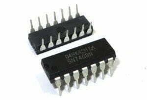
The AT89C51 is a chip based on an 8-bit CMOS microcontroller, manufactured by Atmel, and is also known as the 8051 series microcontroller. It is primarily used in embedded systems, offering advantages such as high flexibility, programmability, and ease of use. It finds applications in various fields such as industrial control, automotive electronics, smart instruments, and has become a significant representative of the MCS-51 microcontroller family.
Introduction to AT89C51 Microcontroller
The AT89C51 is a low-voltage, high-performance CMOS 8-bit microprocessor with 4K bytes of flash programmable and erasable read-only memory (FPEROM). It is manufactured using Atmel’s high-density non-volatile memory technology and is compatible with the industrial standard MCS-51 instruction set and pinout. By combining a versatile 8-bit CPU and flash memory on a single chip, Atmel’s AT89C51 is an efficient microcontroller that provides a flexible and cost-effective solution for many embedded control systems.
Features of AT89C51
- Compatible with MCS-51
- 4K bytes of programmable FLASH memory
- Endurance: 1000 write/erase cycles
- Data retention time: 10 years
- Fully static operation: 0Hz-24MHz
- Three-level program memory lock
- 128×8-bit internal RAM
- 32 programmable I/O lines
- Two 16-bit timers/counters
- Five interrupt sources
- Programmable serial channel
- Low-power idle and power-down modes
- On-chip oscillator and clock circuitry
Functions of AT89C51
1. Data Processing: The AT89C51 has a powerful data processing capability, allowing it to handle various data processing, storage, and transfer tasks. It can perform various data operations using built-in components such as the arithmetic logic unit (ALU), flash memory, and RAM memory.
2. Peripheral Control: The AT89C51 features multiple peripheral interfaces, including general-purpose input/output pins (GPIO), a serial port, SPI interface, and two 16-bit timers/counters, which can be used for communication and control of other hardware devices.
3. Interrupt Handling: The AT89C51 supports various types of interrupts, including external interrupts, timer interrupts, and serial port interrupts. These interrupts enable rapid response to external events and execution of corresponding interrupt service routines.
4. Timing Control: The AT89C51 includes two 16-bit timers/counters that can be used for generating timer interrupts, frequency measurement, pulse width modulation, and other timing-related applications.
5. Programmable Upgrades: Due to its use of flash memory, the AT89C51 can have its program modified through programming, facilitating system upgrades and expansion.
AT89C51 Structure
The internal structure of the AT89C51 microcontroller shows the main functional components inside the chip:

1. An 8-bit central processing unit (CPU) centered around the arithmetic logic unit (ALU) for computation and control.
2. 128 bytes of internal data-accessible memory (internal RAM) with an address range of 00H to 7FH.
3. 21 special function registers (SFRs) distributed in the address range 80H to FFH, used for various control functions.
4. A program counter (PC), a dedicated 16-bit register for storing the address of the next instruction to be executed.
5. 4KB of internal flash memory (on-chip ROM) for storing programs and data.
6. Four 8-bit programmable I/O ports (P0, P1, P2, P3).
7. A UART serial communication port.
8. Two 16-bit timers/counters.
9. Five interrupt sources and a two-level interrupt control system.
10. On-chip oscillator and clock circuitry.
AT89C51 Pin Configuration
The AT89C51 microcontroller has 40 pins categorized into four groups: power, clock, control, and I/O ports.

Power Pins:
– GND (Pin 20): Ground connection.
– Vcc (Pin 40): DC power supply input, typically 5.0V ±20% in the range of -40°C to 85°C, with a maximum rating of 6.6V.
Clock Pins:
– XTAL1 (Pin 19): One of the pins for connecting an external oscillator element, such as a crystal oscillator.
– XTAL2 (Pin 18): The other pin for connecting an external oscillator element.
When using an external oscillator, XTAL1 receives the oscillator’s signal, while XTAL2 is left unconnected. This configuration forms the oscillator, with the frequency determined by the reciprocal of the oscillator’s period.
(Note: The translation is quite detailed. If you prefer a more concise version, please let me know.)
Control Pins:
1. RST (Pin 9): Reset input (used for initialization and restarting).
Reset can occur through two methods: power-on reset and manual reset (by pressing a reset button). It requires that the RST pin remains high for at least 2 machine cycles before transitioning to a low level. This includes a small circuit with resistors and capacitors. The first method is achieved by applying a high voltage to this circuit, while the second method is as simple as pressing a button. Both methods ensure that the RST pin remains high for two machine cycles, completing the reset operation.
2. ALE/PROG (Pin 30): Address latch enable/programming pulse.
This pin, also used as PROG during programming, is employed when downloading programs to the microcontroller. It is related to programming pulses and generates specific waveforms during programming.
3. PSEN (Pin 29): External ROM read signal.
PSEN is related to reading data from external ROM. It acts as a condition for reading data, requiring a valid PSEN signal to successfully read data.
4. EA/Vpp (Pin 31): Internal/external ROM selection/programming voltage.
The 51 microcontroller has 4K of on-chip ROM. If this is insufficient, it can be expanded with external ROM (similar to inserting a memory card in a mobile phone). The value of EA determines whether you are accessing data from internal or external memory. Vpp is used to apply voltage during programming.
Block Diagram of AT89C51 Microcontroller
The following diagram represents the basic functional blocks of the AT89C51 microcontroller. This chip integrates the main components of a microcomputer, including the CPU, memory, programmable I/O ports, timers/counters, serial port, etc. All these components are interconnected through an internal bus.

AT89C51 Vs. 8051 Microcontrollers
8051: Represents the second generation of microcontrollers, belonging to the MCS-51 series. AT89C51: A microcontroller developed by ATMEL that is compatible with MCS-51 and belongs to the third generation of microcontrollers.
MCS-51 microcontrollers refer to a series of microcontrollers produced by Intel in the United States. This series includes 8031, 8051, 8751, 8032, 8052, and 8752. The 8051 microcontroller is the earliest and most typical product in this series. The AT89C51 is based on the core circuitry of the 8051 and was later developed by ATMEL. There are also similar microcontrollers like the STC51, which have the same functionality but are produced by different companies and have different prefixes. In essence, the AT89C51 and the 8051 have identical functionality, but the 8051 is no longer available in the market.
Engineering checks for AT89C51 microcontroller pinout and programming
Before using AT89C51 microcontroller pinout and programming in a PCB, firmware, repair, or validation workflow, confirm the details that usually decide whether the design works reliably instead of only reading the headline specification.
Design and troubleshooting checklist
| Area | What to check | Why it matters |
|---|---|---|
| Minimum circuit | Confirm crystal, reset network, EA/VPP, PSEN, ALE, VCC, GND, and decoupling | Classic 8051 boards fail quickly when reset or oscillator design is weak |
| Memory interface | Check external program/data memory buses, latch timing, and address decoding | AT89C51 systems often depend on correct external bus wiring |
| Firmware access | Document programmer type, lock bits, port usage, and serial communication settings | Repair and cloning workflows need reproducible programming conditions |
These checks help connect the search intent around AT89C51 microcontroller with practical board-level decisions, component selection, and failure analysis.