The LM2596 remains one of the most searched switching regulator parts because it sits in a useful middle ground. It is familiar, widely cloned in module form, and practical for stepping down a higher DC rail to a lower one in embedded and industrial work. When people search for an LM2596 DC-DC buck converter schematic diagram, they are usually trying to understand a module they already bought, design a custom power stage, or debug a board that behaves differently from the textbook drawing.
A good schematic explanation has to do more than identify component names. In a buck converter, the schematic and the layout are tightly connected. You can copy the right functional blocks and still get unstable output, excess heat, audible noise, or poor EMI if the current loops are not treated seriously. So the right way to read an LM2596 schematic is to begin with energy flow and then connect each symbol to a practical board-level consequence.

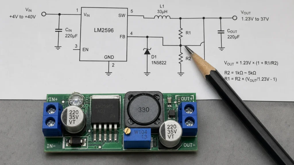
Read the power path from left to right
Most LM2596 schematics are easiest to understand if you ignore part numbers at first and simply follow energy from input to output. At the left side you normally see the input source and an input capacitor. That capacitor is not decorative. It supplies the pulsed current demanded by the switching stage and helps keep the input rail from bouncing. The LM2596 switching regulator IC sits in the middle and rapidly turns current on and off at its switch node. From there, a diode and an inductor shape the current path so the output side receives a smoother, lower DC voltage. Finally, the output capacitor reduces ripple and supports transient load changes.
That basic sequence explains the heart of the circuit: the input capacitor keeps the source side stable, the regulator controls the switching action, the diode provides the current path when the switch turns off, the inductor stores and releases energy, the output capacitor filters the result, and the feedback resistors tell the regulator whether the output is too high or too low.
What each section really does
Input capacitor: The input capacitor handles fast current demand close to the regulator. If it is too far from the IC, has unsuitable ESR, or is undersized for the source condition, the converter may show noisy input behavior or stress the upstream supply.
LM2596 regulator IC: The regulator is the control center. It monitors the feedback voltage and adjusts duty cycle to regulate the output. In practical designs, the surrounding components and layout determine whether the IC can do that job cleanly.
Catch diode: The diode carries inductor current when the internal switch is off. In LM2596 circuits this is usually a fast or Schottky device selected for current, voltage, and recovery behavior appropriate to the design. A poor diode choice can increase heat and reduce efficiency quickly.
Inductor: The inductor influences ripple current, transient response, and saturation margin. If the inductor saturates under load, the converter can become noisy, hot, or unstable.
Output capacitor: The output capacitor smooths voltage ripple and helps the regulator respond to load steps. In real boards, capacitor choice interacts with ESR, temperature range, and expected load profile.
Feedback divider: The feedback network sets the output voltage in adjustable versions and determines what the IC thinks is happening at the load. If you route the feedback path through noisy copper or sample the wrong point on the board, regulation quality can suffer even if every part value is technically correct.
Why copied module schematics often disappoint on custom boards
Many engineers first meet the LM2596 through low-cost module boards. Those modules are useful for prototypes, but they can create a false sense of security. A module often hides component substitutions, thermal compromises, and layout choices that may not translate well into a product.
The common mistake is copying the rough block structure without understanding the critical loops. In a buck converter, the switch node, diode path, and input capacitor loop carry fast-changing current. If those paths become long, narrow, or tangled with signal routing, the board can radiate noise and create measurement confusion. This is why a power schematic should always be reviewed together with PCB layout guidelines rather than in isolation.
A practical example: stepping 12V down to 5V
A classic use case is reducing a 12V input rail to a regulated 5V output for logic, displays, or peripheral electronics. In that scenario, the schematic job is simple on paper but subtle in execution. You want the input capacitor placed close to the regulator input and return path. The diode and inductor should create a compact power stage, not a stretched one. The output capacitor should sit where it can actually support the load side. The feedback sense point should reflect the voltage that matters, especially if the load is several centimeters away or if the output current is significant.
Now consider what happens if the input cable is long, the ground return is weak, or the load current changes sharply. Suddenly the schematic blocks are still correct, but the board may ring, the output may dip, or the regulator may run warmer than expected. That is why power articles that stop at the symbol level are incomplete.
Layout matters almost as much as the schematic
For an LM2596 design, layout is not a cosmetic step after the circuit is done. It is part of the electrical design. Keep the high-current switching loop tight. Use short, wide traces or copper areas where current is substantial. Separate noisy switching regions from sensitive feedback and analog sections. Give the return path a low-impedance route. If the board is heading toward production, review manufacturability early and do not wait until the final design for manufacturing pass to discover that thermal and copper decisions are fighting each other.
This also affects serviceability. Boards that cram the regulator, diode, and inductor into awkward positions are harder to inspect, rework, and validate after PCB assembly. A clean layout reduces both electrical risk and manufacturing friction.
How to test an LM2596 circuit intelligently
When validating the schematic on real hardware, do not jump straight to the output voltage number and stop there. A converter that reads 5V on a multimeter can still be performing badly. Check output voltage under no load and expected load, output ripple with an oscilloscope and proper probing technique, temperature rise on the regulator, diode, and inductor, response when input voltage changes across the expected range, behavior during load steps, and evidence of audible noise or unstable switching.
If a circuit fails, narrow the cause logically. Excess ripple may point to capacitor choice, layout, or current loop size. Heat may indicate bad diode selection, inductor saturation, or an unrealistic module copy. Intermittent behavior can come from feedback routing or poor solder quality in the power path.
Common mistakes to avoid
The same design errors appear repeatedly in LM2596 projects: treating the schematic as complete without reviewing physical current loops, using an inductor with inadequate current margin, picking a diode by voltage alone and ignoring switching behavior, routing feedback through noisy copper, trusting a clone module layout as if it were a reference design, or measuring ripple with poor probing and then chasing the wrong problem.
Final takeaway
An LM2596 buck converter schematic diagram is simple enough to recognize quickly, but it rewards careful reading. The input capacitor, switch stage, diode, inductor, output capacitor, and feedback path each have a clear role. The real engineering work is making those roles cooperate on an actual PCB.
If you understand the current flow first, the symbol set becomes intuitive. If you then pair the schematic with disciplined layout and practical testing, the LM2596 remains a very workable solution for many embedded power rails.
What is the most important section of an LM2596 schematic?
The entire power path matters, but the switching loop around the regulator, diode, input capacitor, and inductor is usually the most critical area for stability, heat, and EMI.
Can I copy an LM2596 module schematic directly into my own PCB?
You can copy the functional topology, but you should not assume a low-cost module is an ideal reference. Review component quality, current limits, thermal behavior, and especially layout before treating it as production-ready.
Why is my LM2596 output noisy even though the voltage is correct?
Correct average voltage does not guarantee clean performance. Output noise can come from poor capacitor choice, long switching loops, inductor saturation, measurement technique, or bad feedback routing.
Does the feedback divider only set output voltage?
Its resistor ratio sets the target voltage, but the feedback path also affects regulation quality. If it samples a noisy point or runs through a poor layout region, the regulator may react to the wrong information.