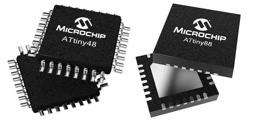
Attiny48/88
The AVR-based ATtiny48/88 microcontroller is a low-power CMOS device that delivers impressive processing power while optimizing power consumption. Its powerful instruction set allows for execution in a single clock cycle, resulting in throughputs that can approach 1 MIPS per MHz.

Features
RISC Architecture
It has an Advanced RISC Architecture with 123 instructions, most of which can be executed in a single clock cycle, and 32 8-bit general-purpose registers.
Memory
The microcontroller operates fully statically and has high durability and non-volatile memory segments. It has 4K/8K Bytes of In-System Self-Programmable Flash program memory (ATtiny48/88), 64/64 Bytes EEPROM (ATtiny48/88), and 256/512 Bytes Internal SRAM (ATtiny48/88).
Peripherals
The microcontroller has a programming lock for software security and a peripheral features section that includes one 8-bit timer/counter with separate prescaler and compare mode, one 16-bit timer/counter with prescaler, and compare and capture modes, an 8-channel 10-bit ADC, a master/slave SPI serial interface, a byte-oriented 2-wire serial interface (Philips I2C Compatible), a programmable watchdog timer with separate on-chip oscillator, an on-chip analog comparator, and an interrupt and wake-up on pin change feature.
I/O lines and Pin
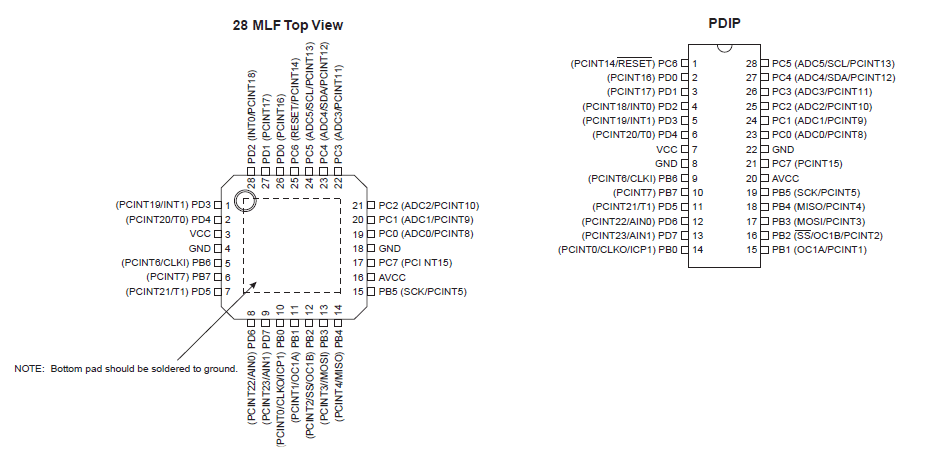
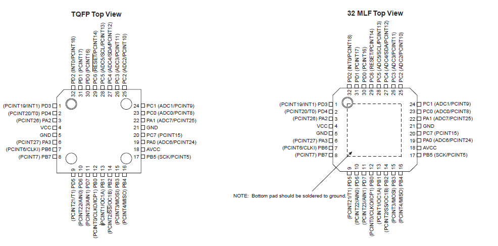
The microcontroller has 28 programmable I/O lines in 32-lead TQFP and 32-pad QFN/MLF package and 24 programmable I/O lines in 28-pin PDIP and 28-pad QFN/MLF package. It also has various operating voltages, a temperature range of -40°C to +85°C, and different speed grades.
Pin Configurations


Block Diagram

With 32 general purpose working registers, the AVR core provides a rich instruction set that offers a range of functionality. All the32 registers are directly connected to the Arithmetic Logic Unit (ALU), allowing two independentregisters to be accessed in one single instruction executed in one clock cycle. The resultingarchitecture is more code efficient while achieving throughputs up to ten times faster than con-ventional CISC microcontrollers.
Comparison Between ATtiny48 and ATtiny88
The ATtiny48 and ATtiny88 are both 8-bit AVR microcontrollers from Atmel. Both of these microcontrollers have a wide range of features, including on-board flash memory, SRAM, EEPROM, and an array of digital and analog peripherals. The following table summarizes the comparison of them:
| Features | ATtiny48 | ATtiny88 |
|---|---|---|
| Program Memory | 4K | 8K |
| EEPROM | 64 bytes | 64 bytes |
| Timer/Counter | 8-bit | 16-bit |
| Analog Comparators | Yes | Yes |
| Built-in USI | Yes | Yes |
| I/O Pins | 28 | 32 |
| ADC Channels | 6 (10-bit) | 8 (10-bit) |
| RAM | 256 bytes | 512 bytes |
| Current Consumption (max) | 4mA | 30mA |
| Operating Voltage | 1.8 – 5.5V | 1.8 – 5.5V |


