About N76E003AT20 Microcontroller
The N76E003 is an 8-bit microcontroller based on the 8051 architecture, with embedded flash memory and rich peripherals. It offers up to 18KBytes of main flash called APROM, which can be used for in-application programming and non-volatile data storage. The LDROM flash, with a maximum size of 4KBytes, is used for the boot code. The microcontroller is equipped with 18 sources of interrupts with 4-level priority capability. The system clock can be switched on-the-fly via software and can be slowed down with a software clock divider for a balance between execution performance and power consumption. It has two power modes, Idle and Power-down, which can be software-selectable to reduce power consumption. Overall, the N76E003 is well-suited for general-purpose, home appliance, or motor control system design.
Features of N76E003AT20 Microcontroller
CPU:
–Fully static design 8-bit high performance 1T 8051-based CMOS microcontroller.
–Instruction set fully compatible with MCS-51.
–4-priority-level interrupts capability.–Dual Data Pointers (DPTRs).
Operating:
–Wide supply voltage from 2.4V to 5.5V.
–Wide operating frequency up to 16 MHz.
–Industrial temperature grade: -40°Cto +105°C.
Memory:
–Up to18KBytesof APROMfor User Code.
–Configurable 4K/3K/2K/1K/0KBytes of LDROM, which provides flexibility to user developed Boot Code.
–Flash Memory accumulatedwith pages of 128 Bytes each.
–Built-in In-Application-Programmable (IAP).
–Code lock for security.
–256 Bytes on-chip RAM.
–Additional 768Bytes on-chip auxiliary RAM (XRAM) accessed by MOVX instruction.
Clock sources:
–16MHz high-speed internal oscillator trimmed to ±1% whenVDD5.0V, ±2% inall conditions.
–10 kHz low-speed internaloscillator.
–External clock input.
–On-the-fly clock source switch via software.
–Programmable system clock divider up to 1/512.
Peripherals:
–Up to17general purpose I/O pins and one input-onlypin.All output pins have individual 2-level slew rate control.
–Standard interrupt pins INT0 and INT1.
–Two16-bit Timers/Counters 0and 1 compatible with standard 8051.
–One 16-bit Timer 2 with three-channel input capture module and 9 input pin can be selected.
–One 16-bit auto-reload Timer 3, which can be the baud rate clock source of UARTs.
–One 16-bitPWM counter interrupt for timer.
–One programmable Watchdog Timer(WDT)clocked by dedicated 10kHzinternal source.
–One dedicated Self Wake-up Timer (WKT) for self-timed wake-up forpower reduced modes.
–Twofull-duplex UART portswith frame error detection and automatic address recognition. TXD and RXD pins of UART0 exchangeable via software.
–One SPI portwith master and slave modes, up to8Mbps when system clock is 16 MHz.
–One I2C bus with master and slave modes, up to400kbps data rate.
–Three pairs, six channels of pulse width modulator (PWM) output,10outputpinscan be selected.,up to 16-bit resolution, with different modes and Fault Brake function for motor control.
–Eight channels of pin interrupt, shared for all I/O ports, with variable configuration of edge/level detection.
–One 12-bit ADC, up to500ksps converting rate, hardwaretriggered and conversion result comparefacilitating motor control.
Power management:
–Twopower reducedmodes: IdleandPower-downmode.
Power monitor:
–Brown-out detection(BOD) with low power mode available, 4-levelselection, interrupt or reset options.
–Power-on reset(POR).
Strong ESD and EFT immunity.
Development Tools:
–Nuvoton On-Chip-Debugger (OCD)with KEILTMdevelopmentenvironment.
–Nuvoton In-Circuit-Programmer (ICP).
–Nuvoton In-System-Programming(ISP)viaUART.
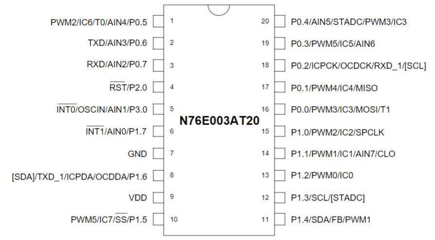
N76E003AT20 Pinout
