PCB Reverse Engineering Services
Table of Contents
What is PCB Reverse Engineering?
PCB Reverse Engineering is the process of disassemble, analyzing, and reconstructing an existing circuit board of electronic devices. It’s typically used for the purpose of duplicating, modifying, or improving the original product. We remove the design data from the physical PCB and convert it into a CAD data format. This allows us to examine it closely and make any necessary adjustments.
Benefits of PCB Reverse Engineering
- You can easily generate your own products and parts without needing the original design measurements or specifications.
- It offers a detailed analysis of existing PCBs, helping manufacturers to better understand the design and components.
- It is a great way to detect defects, analyze failures, and improve the reliability of PCBs.
- It make your products compatible with the components of the competitors’.
- It can help manufacturers reduce costs by helping them access existing parts and components.
- It provides a way to develop compatible systems and integrate the latest technology.
- You can make small modifications to your design easily.
What You'll Get from PCB Reverse Engineering?
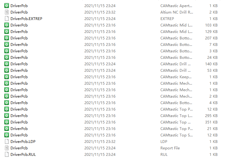
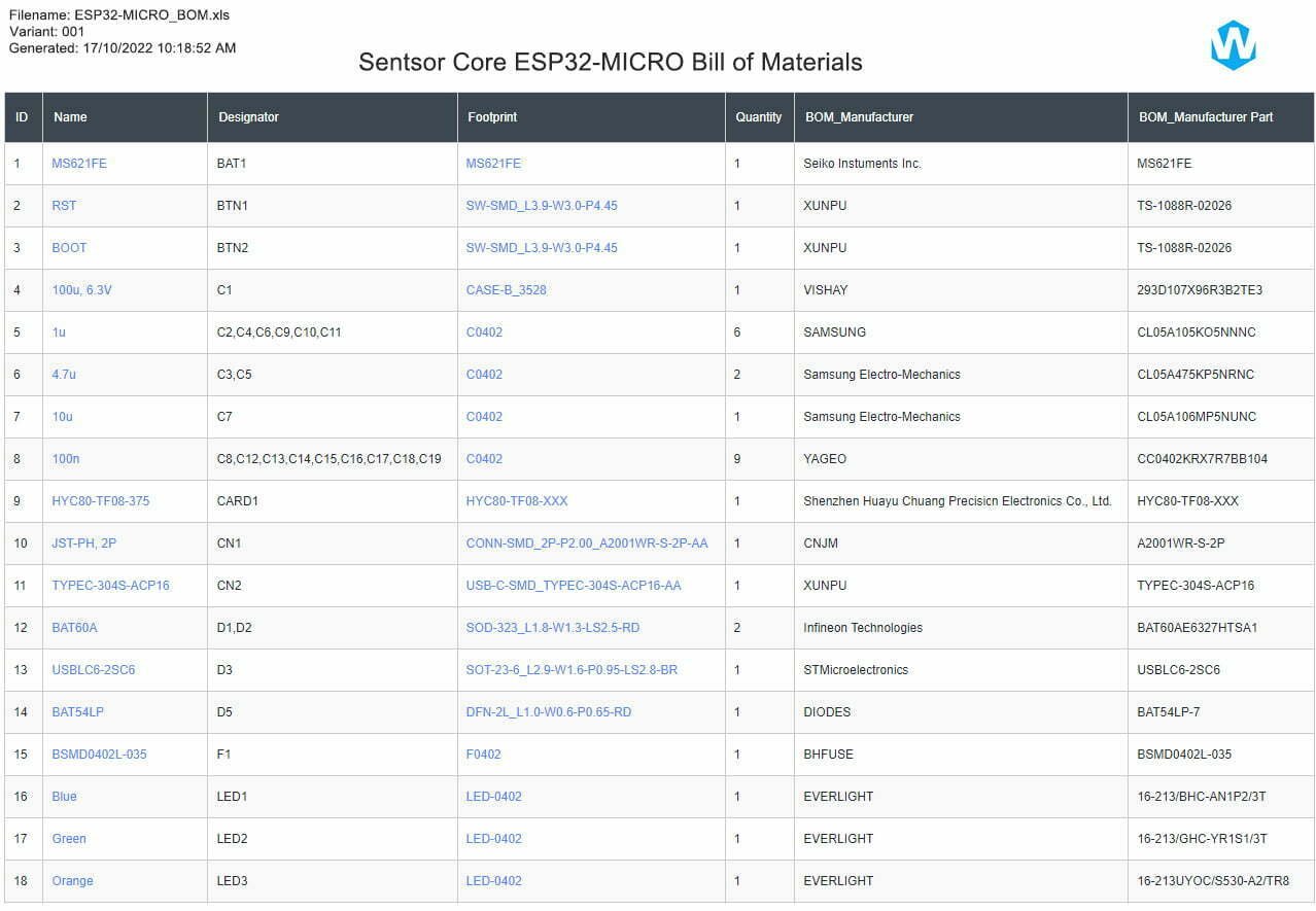
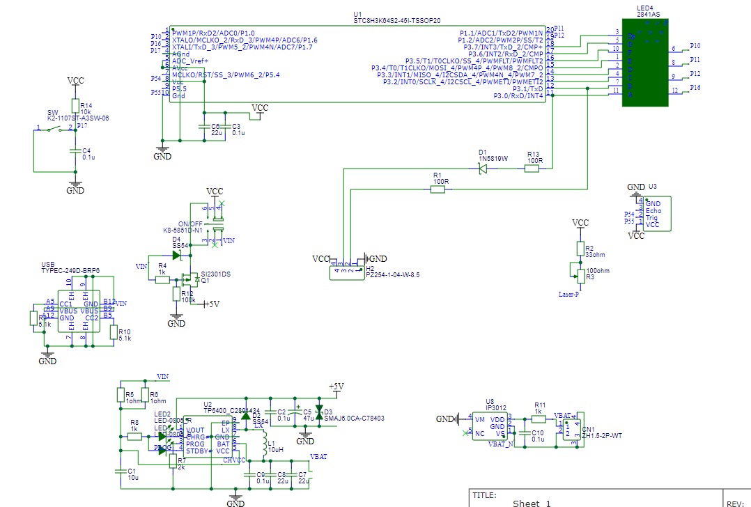
In the situation that there are already physical circuit boards on your electronic devices, we’ll extract or generate the below engineering files for you by reverse engineering:
Based on these engineering files, our engineers can help you achive some more pcb engineerings such as PCB redesign, PCB clone, component soldering, flying probe testing, pcb fabrication and assembly.
How to Reverse Engineer a PCB Board?
It’s important to remember that PCB reverse engineering process can be time consuming and complicated. It might need specialized equipment and knowledge, as well as a thorough understanding of the original design. But with the right process, insights, and resources, you can get the job done correctly. In this guide, we’ll walk you through what it takes to reverse engineer PCBs and support successful projects.

Step #1: Preparing the PCB Sample and Tools
To getting started, you can take some photos of your board and send to us by email. After evaluating your project, we’ll quote back to you. Whatever single-sided PCB, double sided or multilayer, we have faith in realizing your project goal.
Additionally, the reverse engineering also need the necessory pcb software as well as hardware tools. Depending on the complexity of your project, these could include design tools like Eagle, Altium Designer, or DesignSpark. You can find the lists on next setction.
Step #2: Component Recognition and Decoding
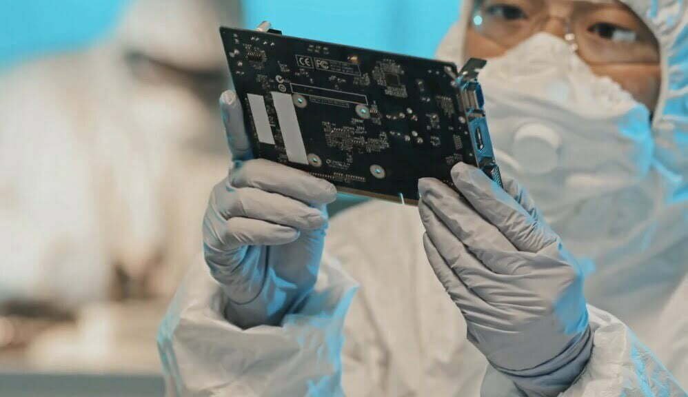
Component recognition and decoding, also known as “component extraction” or “symbol recognition”. The goal of this process is to identify all parts on the board, their respective values, and their associated functions.
We can identify them by comparing the electronic components with reference databases. These databases contain information about the part type, its associated pins, and its functional description.
Step #3: Component Disassembling and BOM Making
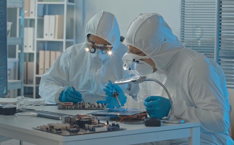
Engineers can disassemble a PCB to get a closer look. They can trace lines and make measurements for further analysis. The disassembly process should be done carefully to avoid damaging the components or the board itself.
Trace the electronic components on the board. This will create a Bill Of Materials (Bom). The Bom lists all components needed to construct the circuit. By tracing components, you can figure out the type and manufacturer of each component on the board, their specifications and prices.
Step #4: PCB Imaging and Scanning
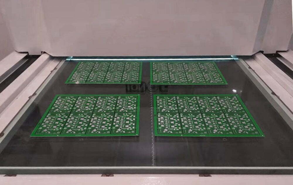
In this step, we need to get high-quality, precise images of the original PCB’s top layer and bottom layer. With these images, we can then trace circuit connections, constructing PCB layout. It’s essential to ensure that the images should contain all the necessary details of the PCB, including the component placement, traces, and any labeling or markings.
We can capture images using various techniques. These include photomicrography, x-ray imaging, and scanning electron microscopy. Each of these techniques offers unique advantages and limitations when examining different types of circuit boards.
Step #5: Images Editing and Uploading
We can enhance the images’ quality and readability with image editing software, such as Photoshop or GIMP. The editing process may involve adjusting brightness, contrast, and color levels to improve the visibility of traces and components. Additionally, image rotation, cropping, and resizing may be necessary to align the images properly.
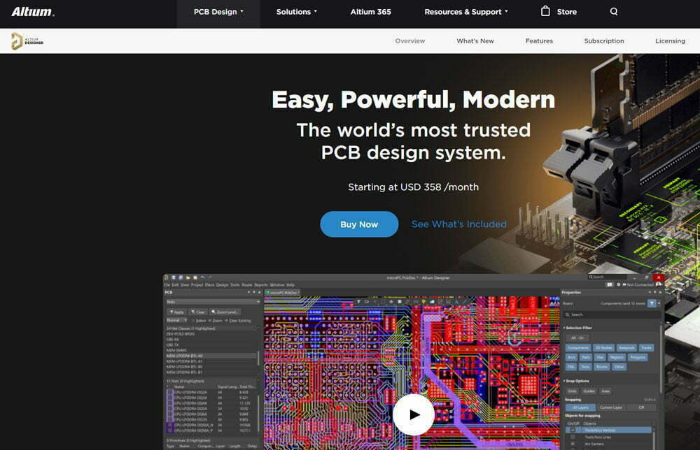
Once the images are edited and finalized, they are typically uploaded to the reverse engineering software or tools for further analysis. There are various software applications available for PCB reverse engineering, such as Altium Designer, Eagle, or KiCad.
Step #6: Circuit Tracing and Layout Constructing
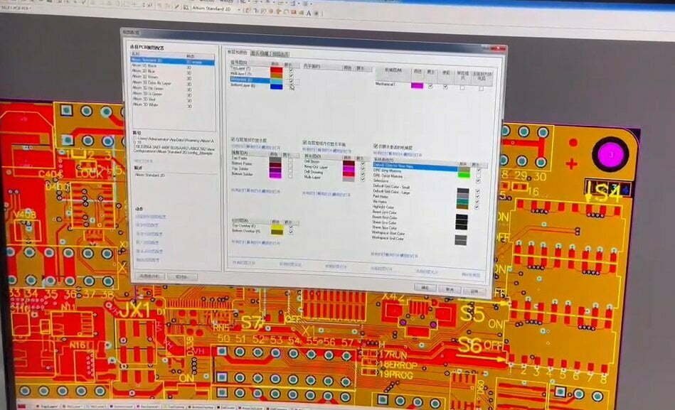
After editing the images, you can upload them to a PCB design software, like AutoTrace, to do circuit tracing and create a layout. This type of program will take the bitmap image and convert it into a vector graphic, helping you obtain the schematic quickly.
Once you have a layout, you’ll then need to save this as a Gerber file. Gerber files are used by PCB manufacturers and semiconductor equipment manufacturers as part of their manufacturing process. They’re used to transfer the layout to manufacturing equipment such as 3D printers and laser cutters.
Step #7: Schematic Creation and Verification
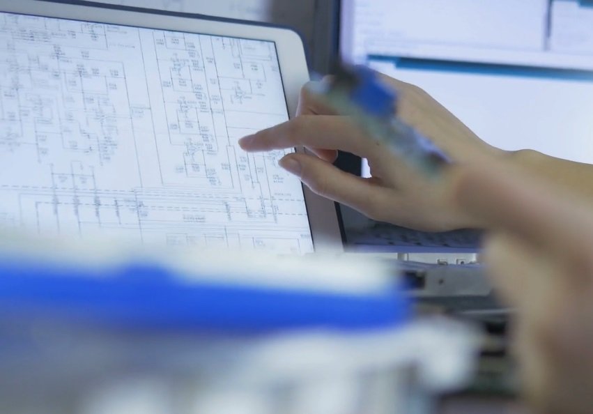
After finishing the layout, the next step is to create the circuit schematic. This involves creating a diagram that represents the circuit connections and the relationship between components. To do this, you’ll need pcb schematic tools like Altium Designer, Eagle, OrCAD, etc.
Next, you’ll need to compare, analyze, and check the schematic diagram against the PCB file diagram. Make sure the schematic diagram and BOM accurately reflect the original design and there’re no any errors.
PCB Reverse Engineering Software
- ScanCAD – support schematic creation, autorouting, and simulation;
- DipTrace – support schematic-based editor or a layout-based editor;
- AutoTrace – a program that automatically converts bitmap images to vector images;
- Protel or Altium Designer – helps you to generate a schematic from a board;
- Gimp – a free and open-source graphics editor for image editing, converting between different image formats;
- Inkscape – a free and open-source vector graphics editor used for creating and editing vector illustrations;
PCB Reverse Engineering Hardware
- A computer – with good performance;
- Digital Camera – photograph the circuit board image;
- Multimeter – to measure voltage, current, and resistance so that you can identify the components ;
- A hot air rework station – to remove and replace components;
- A soldering iron and solder – to attach and detach wires;
- Microscope – to inspect the board and components;
- A magnifying glass – to identify components with printed symbols on the board;
Applications of PCB Reverse Engineering
Industry:
Product improvement and redesign, legacy system maintenance, failure analysis and troubleshooting.
Automotive:
Replicate circuit boards in car electronics such as dashboard displays and engine control units.
Medical Devices:
Analyze and redesign circuit boards in medical equipment such as MRI machines and pacemakers.
Consumer Electronics:
Recreate obsolete products, such as retro gaming consoles, computer motherboards, monitoring equipment.
Multi-Layer PCBs Reverse Engineering
Step 1: Prepare a Multi-Layer PCB
- Get a good circuit board and identify components in high positions.
- Record component details before disassembling.
- Scan the board at High DPI resolution.
- Clean the PCB surface before scanning to ensure clear visibility.
Step 2: Disassemble Components and Create BOM
- Use an air gun and tweezers to remove components.
- Record component information on a prepared table.
- Measure component values with a bridge.
- Input measurement data to the computer for archiving.
Step 3: Remove Tin on the Surface
- Use flux and a soldering iron to remove tin dross.
- Adjust the soldering iron’s temperature based on the PCB layers.
- Wash the board and dry it after removing tin.
Step 4: Make Clear PCB Bottom Map
- Set scanned images as top and bottom layers.
- Convert images for various copying software.
- Package and position components accurately.
- Remove all the coating layers on the surface.
- Ensure a clear and complete PCB bottom map.
Step 5: Create a Schematic Diagram or layout
- Research the datasheets of the identified chips and components.
- Use software like Altium Designer or Eagle.
- Trace connections and identified components.
- Create the components and their connections.
Step 6: Inspect the Schmatic and Fabricate Prototype
- Use software to verify and modify the accuracy of schematic.
- Perform precision adjustment correction as needed.
- Fabricate a prototype PCB using the reverse-engineered schematic.
- Test the performance of reverse-engineered PCB.
Best Practices for PCB Reverse Engineering
Separate Functional Areas
To make drawing a PCB's schematic diagram easier and avoid unnecessary problems, engineers can separate functional areas when reverse designing it. Usually, on a PCB, electronic components with similar functions are placed together. By separating functional areas, engineers can efficiently draw a PCB's schematic diagram during reverse design.
Find the Reference Parts
To get started, we should find the reference parts, and then drawing schematic basing on their pins. This helps to ensure the highest possible accuracy of the schematic. The reference parts are generally larger in size and have more pins, which are convenient for drawing. Examples of suitable reference parts include integrated circuits, PCB transformers, and transistors.
Learn from Similar Schematic
To create electronic circuits, engineers should be skilled in designing the basic circuit frames and schematics. The similar electronic products often have comparable schematic diagrams. With prior experience, engineers can use similar circuit diagrams to reverse engineer new product schematics.
Development Trends of PCB Reverse Engineering
In past 40 years, there were many technology continues to evolve for PCB reverse engineering. Here are some of the latest developments:
- Advanced Imaging Techniques: the high-resolution cameras or mobile phone can now clearly photograh images of PCBs.
- X-Ray Technology: X-rays can penetrate through multiple layers of a PCB, allowing reverse engineers to see the internal components and connections.
- Artificial Intelligence: AI can assist with image processing and analysis, helping us identifing components and connections on a PCB.
- 3D Printing Technology: It allows designers to create a physical model of the circuit board design, which can be used for testing and verification purposes.
FAQ about PCB Reverse Engineering
Is PCB reverse engineering legal?
As a method of technological innovation, reverse engineering has always been controversial. On the one hand, reverse engineering violates copyright, while on the other hand it restricts technology monopoly and promotes healthy competition in technology.
Copyright law and the Digital Millennium Copyright Act (DMCA) are important regulations related to reverse engineering. Some claim that unofficial versions of software programs created during reverse engineering are themselves a violation of copyright law. However, the court did not think so. Reverse engineering may be permitted even in violation of trade secrets or copyright. As long as the reverse engineering is used to:
Develop competing products
Improve product features
Fix Security Vulnerabilities
Interoperate with other products
Therefore, if you are considering reverse engineering a product, it is important that you understand the local laws.
What are the costs of PCB reverse engineering?
| Circuit Board Size | Complexity | Approximate Cost Range |
|---|---|---|
| Small (2″x2″ or smaller) | Without complicated features or parts, with instructions | $500 - $1,500 |
| Middle-sized or double-layer (up to 6″x6″) | Some complexity and components | $1,500 - $5,000 |
| Large multi-layer (larger than 6″x6″) | High complexity | $5,000 - $20,000 or more |
How long does it take for my project?
The time to complete a PCB reverse engineering project depends on its complexity, layers of the pcb, availability of reference materials, etc. A simple project can take a few days or weeks, while a complex one can take several weeks or months.
Contact Us
Room 711, Building 4, Phase 2, Dongjiu Innovation Technology Park, No. 73 Xialinan Road, Nanwan Street, Longgang District, Shenzhen, China.

