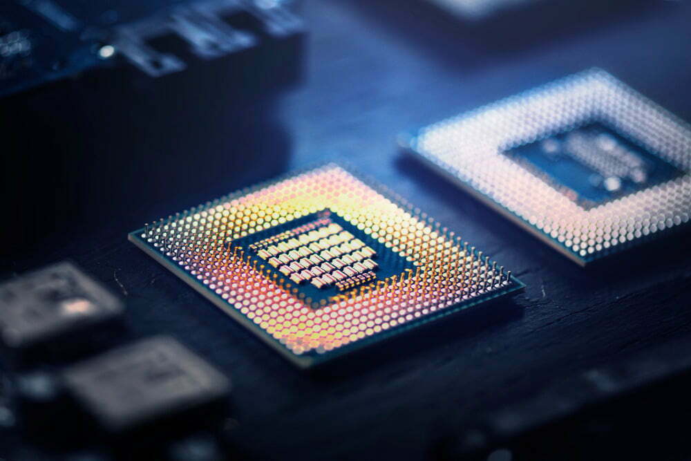
What is IC Reverse Engineering?
IC Reverse engineering is the process of learning about its inner workings by extracting, examining, and classifying its circuits.
Benefits of IC Reverse Engineering
There are a number of reasons why someone might want to reverse engineer an IC. For example, they may be trying to improve upon the design, create a compatible replacement part, or understand how a particular IC works in order to design a better one.
improve upon the design, to create a knock-off product, or to diagnose a problem;
– Identify potential issues with a product before it goes to market;
– Develop a better understanding of how a product works;
– Improve upon the design of a product;
– Create a replica of a product;
– Analyze a competitor’s product and find out how it works;
– Create custom versions of products for specific customer needs.
How to Reverse Engineering ICs?
Step1: Gather all the required equipment
The first step in IC reverse engineering is to prepare all required tools or software:
– Design tools: cadence, synopsys, mentor, Altera, Xilinx, Keil Software;
– Layout extraction tools: NetEditorLite, ChipAnalyzer;
– Algorithm design tools: MATLAB;
– PCB layout tools: Altium Designer, Orcad, Allegro;
Step2: identify the circuit elements
Next, we identify the circuit elements that make up the IC. This can be done by looking at the IC under a microscope or by using special software to analyze the IC’s structure. Once the circuit elements have been identified, the next step is to determine their function. This can be done by observing the IC in action or by using simulation tools to test different hypotheses.
Step3: Take a photograph of the original ICs
Please make sure take a high pixel pictures of IC, or it’ll affect the later accuration of creating layout.

Step4: Create a layout of the chip
Then use image recognition software to convert the image into data and creat a layout. Image recognition software enables engineers to reverse engineer ICs by “reading” an image and converting the pixels of the image into data. Once the data is collected, the software turns it into vectors, which are the points that make up the image. Then, the software converts the vectors into data and creates a layout.
The layout of the chip must be in the same position as in the original photograph. The edges of the chip should be marked with a pen or highlighter. It is necessary to take into account the perspective of the photo and its angle. If the angle is not correct, the layout will be incorrect. After marking the chip’s edges, you must take a photograph of the layout. Make sure that there are no shadows on the chip. Shadows can distort the image and make it unusable. After the image is saved, you can use it for the next steps.
Step5: Extract the circuit netlist from the layout
This process is similar to extracting the schematic netlist. If a layout is imported from a format such as AutoCAD, it must be converted to a format that is understood by the extraction software. Converting the layout may include converting units, dimensions, layers, and other properties. The extracted layout is represented as a netlist, which is a data structure used to describe a circuit design.

Step6: Use the netlist to create a schematic of the circuit
Once the functions of the circuit elements have been determined, the next step is to create a schematic diagram of the IC. This diagram will show how the different elements are interconnected and will be used to understand the IC’s overall functionality. Finally, the last step is to create a layout diagram, which shows the IC’s physical layout. This is important for understanding how the IC is manufactured and for identifying potential problems with the design.
Related Post