In the era of AI servers, 5G smartphones, and autonomous vehicles, the performance of a chip is only as good as the “nervous system” supporting it—the IC substrate. As circuit density reaches its physical limits, the choice of fabrication process determines the signal integrity and reliability of the final product.
Today, three primary “sculpting tools” dominate the industry: Tenting (Subtractive), mSAP (Modified Semi-Additive Process), and SAP (Semi-Additive Process). This guide breaks down their technical mechanics, pros and cons, and where they fit in the modern electronics ecosystem.
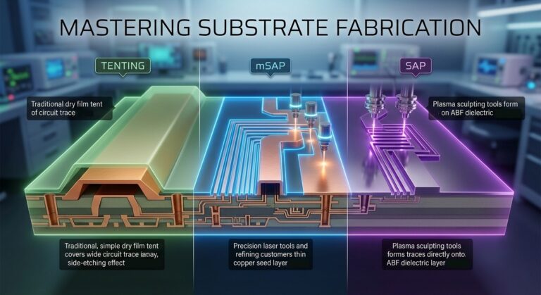
1. Tenting Process (Subtractive Method)
The Tenting process is the most traditional and widely used line-forming technology in the PCB and low-density substrate industry. Its core philosophy is “cover and remove”—much like carving a seal from a block of stone.
How it Works: It starts with a Copper Clad Laminate (CCL) with a thick copper foil (usually $> 12\mu m$). A dry film (photoresist) covers the intended circuit areas like a “tent” over the holes (hence the name). Unprotected copper is then chemically etched away.
The Problem (Side Etching): Because etching removes copper vertically and horizontally simultaneously, it creates a “trapezoidal” cross-section. This “side etching” limits the precision of the line width and space ($L/S$) to roughly $30\mu m/30\mu m$.
Best For: Standard consumer electronics, automotive PCBs, and traditional Wire Bond BGA (WB BGA) substrates.

2. mSAP (Modified Semi-Additive Process)
As pin counts grew and signals sped up, mSAP emerged as the bridge between traditional PCBs and high-end IC substrates. It is currently the mainstream choice for FCBGA substrates used in network chips and premium smartphone processors.
How it Works: Instead of thick copper, mSAP starts with an ultra-thin copper base (usually $3$–$5\mu m$) or a chemically deposited “seed layer”. Circuitry is “added” via selective electroplating to the desired thickness.
The Advantage: After plating, a quick “flash etching” removes the ultra-thin base layer. Since the base is so thin, the etching time is minimal, resulting in nearly vertical, rectangular circuit walls with $L/S$ capabilities down to $10\mu m/10\mu m$.
Best For: High-end smartphone APs (Apple A-series, Snapdragon), Chip Scale Packaging (FCCSP), and Substrate-like PCBs (SLP).

3. SAP (Semi-Additive Process)
SAP represents the pinnacle of circuit precision, often referred to as a “purified” version of mSAP. It abandons copper foil entirely in favor of “pure addition”.
How it Works: It utilizes a copper-free dielectric material, most notably ABF (Ajinomoto Build-up Film). A microscopic “seed layer” ($< 1\mu m$) is chemically deposited on the smooth surface, followed by selective plating to build the circuits.
The Advantage: Since the seed layer is almost non-existent, etching has zero impact on the circuit morphology. This allows for extreme precision ($L/S < 10\mu m$) and superior impedance control for high-speed signals.
Best For: High-performance computing (HPC), AI accelerators (Nvidia H100), and advanced packaging like CoWoS and HBM.

4. Comparison Table: Tenting vs. mSAP vs. SAP
| Feature | Tenting | mSAP | SAP |
|---|---|---|---|
| Core Principle | Subtractive: Etch away thick copper foil | Additive: Plate over ultra-thin copper base | Pure Additive: Seed layer on copper-free dielectric |
| Line Precision (L/S) | > 30μm | 10μm - 30μm | < 10μm |
| Cross-section Shape | Trapezoidal (Side-etching) | Near-Rectangular | Perfectly Rectangular |
| Base Material | Standard CCL | Ultra-thin copper foil | ABF (Ajinomoto Build-up Film) |
| Primary Application | Consumer PCBs / Motherboards | Smartphone AP / High-end HDI | AI Accelerators / CPU / GPU Substrates |
| Cost & Maturity | Low Cost / Highly Mature | Medium-High / Mainstream High-end | Very High / Cutting-edge |
Looking Ahead: The Future of Fabrication
The industry is moving toward a “hybrid” approach to balance cost and performance—using Tenting for core layers and mSAP/SAP for high-density outer layers. As AI demand pushes the boundaries of Moore’s Law, emerging technologies like glass substrates and embedded die will continue to evolve alongside these three fundamental processes.
Understanding the nuances of these fabrication methods is the first step in mastering the complex landscape of modern chip packaging and hardware security.