SWD and JTAG are popular debugging interfaces for those MCU basing on Cortex-M. But these two interfaces are different in both structure and applications. In this article, we’ll introduce their pins, working principle, Pros and Cons.
SWD Interface
SWD, Serial Wire Debug, is a protocol designed by ARM for programming and debugging their microcontrollers. It is based on the ARM CoreSight debugging architecture and enables reading and writing of chip registers through data packets. SWD is a two-wire protocol for accessing ARM debugging interfaces. It is part of the ARM Debug Interface Architecture Specification and serves as an alternative to JTAG. In cases where PCB layout is limited and pin resources are constrained, SWD is a good choice. Many debuggers in the market support SWD debugging interfaces, such as ST-Link, J-Link, e-Link, GD-Link, and others.

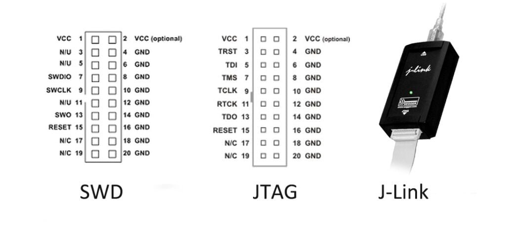
SWD Pins
SWDIO: Serial Wire Data Input Output, serial data input and output pin
SWCLK: Serial Wire Clock, serial line clock pin
For SWDIO, it is a bidirectional (input and output) data pin, and the line must be pulled up on the circuit board (ARM recommends 100 K).
How SWD Work?
External devices, like debug probes, connect to SWDIO/SWCLK to access the Serial Wire Debug Port (SW-DP) directly. SW-DP can access one or multiple Access Ports (APs), and through APs, the rest of the system’s registers can be accessed. An important AP for Cortex M-series CPUs is the AHB-AP, which serves as the master on the internal AHB bus. In other words, AHB-AP can access the memory map of the internal core. Since internal flash, SRAM, debug components, and peripheral devices are all memory-mapped, AHB-AP can control the entire device, including programming it. The entire SWD operation process is hierarchical, with clock signals input from the SWCLK pin, and data signals input/output from the SWDIO pin. Initially, the debugger operates on the SW-DP to determine the parameters of AP registers, allowing manipulation of the Cortex Memory Map.
Advantages of SWD
- Reduced Signal Count
- Reliability at High Speeds
- Reduced Probability of Failures
- Compatibility with JTAG Simulations
- Requires fewer pins for operation
JTAG Interface
JTAG, Joint Test Action Group, was originally used to test chips. This group initiated discussions in the late 1980s and formally released documents interpreting IEEE standards in 1990. (IEEE stands for the Institute of Electrical and Electronics Engineers, an international organization responsible for publishing standards like WiFi and Bluetooth.) The protocol they proposed was documented in IEEE 1149.1 in 1990. This document has since undergone revisions and improvements, with the latest standard as of the time of this writing being IEEE 1149.7.

JTAG Pins
- TDI: Test Data In, a serial input pin.
- TDO: Test Data Out, a serial output pin.
- TCK: Test Clock, a clock pin.
- TMS: Test Mode Select, a mode selection (control signal) pin.
- TRST: Test Reset, a reset pin.
How JTAG Work?
The principle of JTAG involves defining a Test Access Port (TAP) within the device. This allows testing of internal nodes using specialized JTAG test tools. JTAG testing enables multiple devices to be connected in series through a JTAG interface, forming a JTAG chain for individual device testing. Nowadays, JTAG interfaces are also commonly used for In-System Programmable (ISP) operations, such as programming FLASH devices. In terms of hardware structure, the JTAG interface consists of two parts: the JTAG port and the controller. Devices compatible with the JTAG interface can be microprocessors (MPUs), microcontrollers (MCUs), PLDs, CPLDs, FPGAs, DSPs, ASICs, or other chips compliant with IEEE 1149.1 specifications. IEEE 1149.1 mandates the presence of a shift register unit called the Boundary Scan Unit (BSU) for each pin of a digital integrated circuit chip. It connects the JTAG circuit with the core logic circuit while isolating the core logic circuit from the chip’s pins. All of the chip’s Boundary Scan Units constitute the Boundary Scan Register (BSR). The Boundary Scan Register circuit is active only during JTAG testing and does not affect the chip’s functionality during normal operation.
The JTAG protocol controls the transition of the TAP state machine through the TMS signal. After system power-up, the TAP controller first enters the Test-Logic Reset state, then sequentially transitions through Run-Test/Idle, Select-DR-Scan, Select-IR-Scan, Capture-IR, Shift-IR, Exit1-IR, and Update-IR states before returning to Run-Test/Idle. During this process, state transitions are driven by the TCK signal (rising edge), with TMS signals used to select the TAP state. In Capture-IR state, a specific logic sequence is loaded into the instruction register; in Shift-IR state, a specific instruction can be shifted into the instruction register; and in Update-IR state, the instruction just entered into the instruction register is used to update the instruction register. Finally, the system returns to the Run-Test/Idle state, where the instruction takes effect, completing access to the instruction and registers. After returning to the Run-Test/Idle state, based on the content of the instruction register, the required data register is selected, and work on the data registers begins.
Advantages of JTAG
- JTAG is not limited to ARM chips; it is supported in chips beyond ARM, such as the well-known MSP430.
- JTAG has a wide range of applications for programming, debugging, and production testing.
- JTAG is an independent group that evolves with the development of the protocol.
Engineering checks for SWD and JTAG debug interface selection
Before using SWD and JTAG debug interface selection in a PCB, firmware, repair, or validation workflow, confirm the details that usually decide whether the design works reliably instead of only reading the headline specification.
Design and troubleshooting checklist
| Area | What to check | Why it matters |
|---|---|---|
| Pin budget | Compare SWDIO/SWCLK/NRST with TMS/TCK/TDI/TDO/TRST requirements | SWD saves pins while JTAG can support scan-chain workflows |
| Board access | Place keyed headers or pads with ground reference, target voltage, and reset control | Debug reliability depends on physical access as much as protocol choice |
| Security | Plan debug lock, readout protection, boundary scan needs, and recovery procedures | Production security can conflict with repair and failure-analysis access |
These checks help connect the search intent around SWD vs JTAG with practical board-level decisions, component selection, and failure analysis.
Conclusion
JTAG and SWD are both important embedded system debugging interfaces, each with its own strengths and weaknesses. The choice of interface depends on project requirements, hardware support, and performance needs. For complex systems, JTAG may be necessary to gain more control and functionality, while SWD may be a better fit for resource-constrained systems. Considering these factors collectively can help you make informed decisions for more effective embedded system development and debugging.