STM8S003F3P6 Description
STM8S003F3P6 is a microcontroller unit (MCU) developed by STMicroelectronics. It is a highly integrated device that combines the processing power of a central processing unit (CPU) with memory, input/output interfaces, and other peripherals on a single chip. The STM8S003F3P6 is based on an 8-bit architecture and provides a wide range of features, making it suitable for a variety of applications. It has a flash memory of 8KB, 1KB of RAM, and 128 bytes of EEPROM. It also has a wide range of communication interfaces such as SPI, I2C, UART, and CAN. The STM8S003F3P6 is widely used in applications such as industrial control systems, automotive electronics, consumer electronics, and more.
STM8S003F3P6 Pinout

STM8S003F3P6 Features
Core
- 16 MHz advanced STM8 core with Harvard architecture and a 3-stage pipeline
- Extended instruction set
Memory
- 8 Kbytes of Flash program memory
- 1 Kbyte of RAM
- 128 bytes of true data EEPROM, rated for up to 100,000 write/erase cycles
Clock, reset, and supply
- 2.95 V to 5.5 V operating supply
- Internal user-trimmable 16 MHz RC and internal low-power 128 kHz RC clock sources
- Clock security system, watchdogs, brown-out reset, and low-power modes
Peripherals and development
- 16-bit advanced-control and general-purpose timers, an 8-bit basic timer, and an auto-wakeup timer
- UART, SPI up to 8 Mbit/s, and I²C up to 400 Kbit/s
- 10-bit ADC with up to five multiplexed channels on STM8S003F3 devices
- Single-wire interface module (SWIM) for programming and non-intrusive debugging
STM8S003F3P6 Parameters
| Attribute | Value |
|---|---|
| Program memory size | 8KB |
| Data bus width | 8 bits |
| ADC resolution | 10 bits |
| Maximum clock frequency | 16 MHz |
| Number of inputs/outputs | 16 inputs/outputs |
| Data RAM size | 1KB |
| Supply voltage - min | 2.95 volts |
| Supply voltage-max | 5.5V |
| Minimum operating temperature | -40 degrees Celsius |
| Maximum operating temperature | +85 degrees Celsius |
| Data RAM Type | Memory |
| Data ROM size | 128B |
| Data ROM Type | EEPROM |
| Interface Type | I2C, SPI, UART |
| Number of ADC channels | 5 channels |
| Number of timers/counters | 3 timers |
| Operating supply voltage | 2.95V to 5.5V |
| Processor family | STM8S |
| Program memory type | STM8S Flash memory |
| Unit weight | 191 mg |
Block Diagram

STM8S003F3P6 Schematic
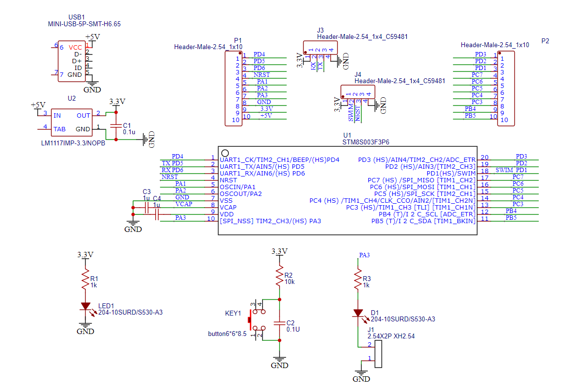
Engineering checks for STM8S003F3P6 pinout, schematic, and programming
Before using an STM8S003F3P6 in a PCB, firmware, repair, or validation workflow, verify the exact TSSOP-20 pinout and the board-level requirements instead of relying only on family-level specifications.
STM8S003F3P6 Power, Pinout, and Debug Checks
| Area | What to check | Why it matters |
|---|---|---|
| Minimum circuit | Provide VDD, VSS, NRST, SWIM, local decoupling, and a stable supply close to the MCU | Power integrity and reset wiring must be correct before firmware or peripheral debugging is meaningful |
| Pin multiplexing | Reserve ADC, timer, UART, I²C, SPI, and GPIO functions before assigning connector pins | The TSSOP-20 package requires tradeoffs between programming access and application I/O |
| Factory flashing | Expose SWIM, NRST, ground, and power test pads with clear polarity marks | Production boards need repeatable programming and recovery after assembly |
Official ST references:
- STM8S003F3 product page — status, package options, and official documentation
- STM8S003F3/K3 datasheet (DS7147) — pinout, electrical limits, memory, clocks, and peripherals
- STM8S/STM8AF reference manual (RM0016) — registers, peripherals, SWIM, and programming behavior
Conclusion
The STM8S003F3P6 is recognized for its ability to safeguard the Flash program memory and data EEPROM against accidental memory overwrites caused by software malfunctions. And there are two levels of write protection.
In addition, this write protection can be removed by writing a large number of key sequences in the control registers in order to perform in-application programming (IAP), which allows the application to modify the contents of the main program memory and data EEPROM, or to reprogram the device option bytes. Its security and reliability is very high.