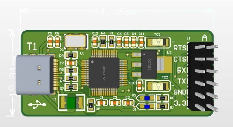
In the world of electronic device manufacturing, the Printed Circuit Board (PCB) plays a crucial role as the foundational component, providing electrical connections and mechanical support for electronic components. However, the surface finish of the PCB is equally vital, as it directly impacts the performance, reliability, and longevity of the circuit board. This article delves into the various PCB surface finishes and provides insight into how to select the most suitable finish for different applications.
Hot Air Solder Leveling (HASL)
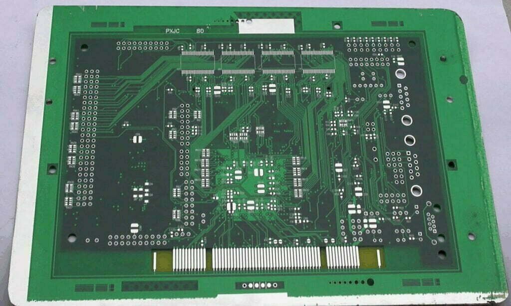
Hot Air Solder Leveling (HASL) is one of the most commonly used surface finishes in the PCB industry. This process involves coating the PCB surface with molten tin-lead solder and then using heated compressed air to level the solder, forming a coating that protects the copper from oxidation and provides excellent solderability.
Advantages
- Abundant material supply
- Reworkable
- Long shelf life
- Excellent solderability
Disadvantages
- Potentially uneven surface
- Not suitable for fine-pitch applications
- Risk of thermal shock and solder bridging
HASL is often chosen for its reliability and ease of use, though it may not be ideal for high-density applications due to its surface irregularities.
Immersion Tin (ImSn)
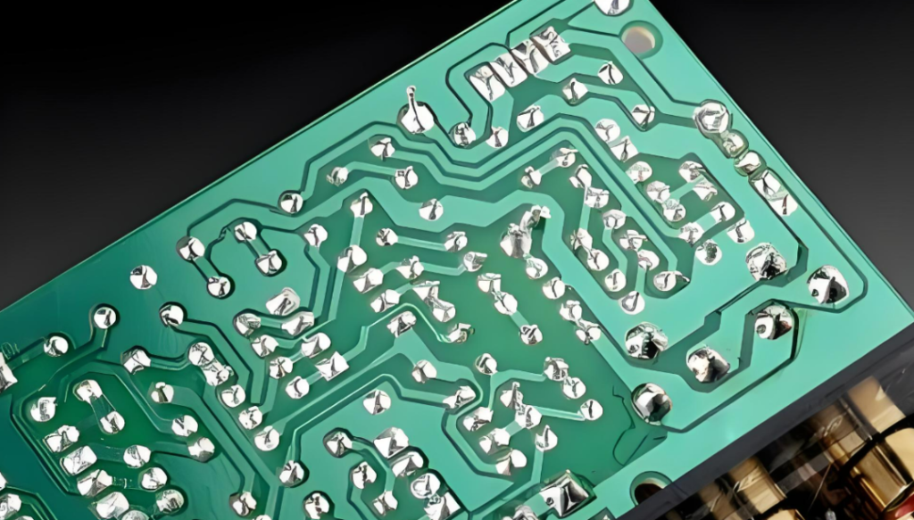
Immersion Tin involves a chemical displacement reaction that deposits a layer of tin onto the PCB’s copper substrate. This finish protects the copper from oxidation and provides a surface that is compatible with a variety of solder types.
Advantages
- Excellent planarity
- Suitable for fine-pitch and SMT
Disadvantages
- Sensitive to handling
- Shorter shelf life
- Potential for corrosion of the solder mask
Immersion Tin offers superior flatness, making it ideal for applications requiring fine-pitch components, though it comes with handling challenges and shorter durability.
Electroless Nickel/Immersion Gold (ENIG)
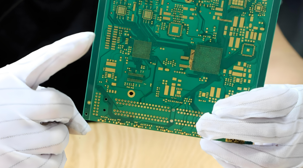
ENIG is a two-step process where a thin layer of nickel is first applied, followed by a layer of gold. The nickel layer acts as a barrier to copper, while the gold layer protects the nickel from oxidation and corrosion, making it an excellent choice for long-term reliability.
Advantages
- Flat surface
- Lead-free option
- Excellent shelf life
- Ideal for fine-pitch applications
Disadvantages
- Higher cost
- Non-reworkable
- Potential for signal loss in RF circuits
ENIG is well-suited for high-performance applications, especially those that require fine-pitch components, but its cost and non-reworkable nature may be limiting factors.
Organic Solderability Preservative (OSP)
OSP is a thin protective layer applied to exposed copper, providing oxidation resistance and protection against environmental factors like moisture and thermal shock. This coating can be easily removed during soldering, ensuring that the copper surface is ready for welding.
Advantages
- Simple and cost-effective
- Suitable for lead-free soldering
- Ideal for horizontal production lines
Disadvantages
- Thickness is difficult to measure
- Not suitable for electroplated through-holes (PTH)
- Relatively short shelf life
OSP is a low-cost solution for standard applications, though its limitations in terms of durability and the need for precise handling make it less suitable for more complex designs.
Immersion Silver
Immersion Silver is a non-electrolytic chemical surface treatment where silver ions are deposited onto the copper surface. This finish is known for its excellent electrical performance, making it ideal for EMI shielding, dome switches, and wire bonding.
Advantages
- RoHS-compliant and environmentally friendly
- Good electrical performance
- Suitable for high-temperature, high-moisture environments
Disadvantages
- High storage requirements
- Susceptible to contamination
- Limited assembly window after removal from packaging
Immersion Silver provides a reliable and eco-friendly solution for various high-performance applications, though its storage and contamination issues can pose challenges.
Electroless Nickel/Electroless Palladium/Immersion Gold (ENEPIG)
ENEPIG involves a copper-nickel-palladium-gold layered structure, offering exceptional flatness and superior soldering performance. The palladium layer between the nickel and gold acts as an additional corrosion barrier, ensuring long-lasting reliability.
Advantages
- Extremely flat surface
- Multiple cycle assemblies possible
- Long shelf life (up to 12 months or more)
Disadvantages
- Relatively expensive
- Limited reworkability
ENEPIG is ideal for high-precision applications, especially where long-term reliability is required. However, its higher cost and limited reusability make it less ideal for mass production environments.
Hard Gold (Electrolytic Hard Gold)
Hard Gold plating, also known as electrolytic gold, is a durable surface finish used for areas that experience high wear, such as edge connectors. The gold plating typically ranges from 99.6% to 99.9% purity and provides robust protection against corrosion and wear.
Advantages
- High durability and wear resistance
- Ideal for high-traffic areas like connectors
Disadvantages
- Higher cost
- Limited to specific high-wear applications
Hard Gold is best for applications where long-term physical durability is critical, though it is not suitable for general-purpose PCB designs due to its high cost and specialized use.
Conclusion
Choosing the right PCB surface finish is crucial for ensuring the performance, reliability, and longevity of electronic devices. Each surface treatment has its own set of advantages and limitations, making it essential to select the appropriate process based on the specific requirements of the application. Factors such as component density, environmental conditions, cost considerations, and the desired shelf life all play a role in determining the best surface finish for your PCB.

