
Gerber Files Explained: Definition & Use Guide
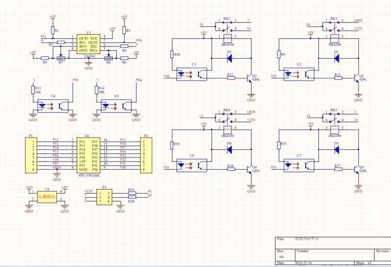
Gerber files for PCBs: formats, layers, and why they’re critical for manufacturing. Learn to generate and verify files with Eagle/Altium. Step-by-step guide!
Gerber files for PCBs: formats, layers, and why they’re critical for manufacturing. Learn to generate and verify files with Eagle/Altium. Step-by-step guide!
Master schematic design: component placement, netlisting, and error-free layouts. Tips for symbol creation, hierarchy, and collaboration with Altium/Eagle. Read now!