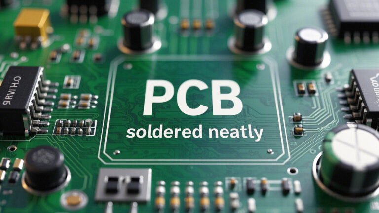
PCB (Printed Circuit Board) mounting. The bane of some engineers’ existence and a therapeutic exercise for others. Let’s be honest, it’s not brain surgery. We’re not splitting atoms or mapping the human genome here. But, like any skill, it requires a modicum of planning, patience, and a healthy respect for hot metal. Fail to heed the warnings, and you might find yourself with a smoking board and a very expensive paperweight. This article aims to gently guide you through the process, highlighting common pitfalls and offering (hopefully) helpful advice.
We’ll break down the process into manageable chunks, from intelligently arranging components to applying just the right amount of solder. We’ll even touch upon the exciting world of “smoke testing,” a rite of passage for any electronics enthusiast. Consider this your friendly guide to avoiding catastrophic PCB mounting failures. So grab your soldering iron, your magnifying glass, and your sense of humor, and let’s dive in!
Prepare to embark on a journey where electronic components find their designated homes on a green canvas, connected by a network of conductive pathways. We’ll explore the intricacies of component placement, the art (and science) of soldering, and the nerve-wracking moment of powering up your creation for the first time. Fasten your seatbelts, because this is going to be a wild ride through the world of PCB mounting.

PCB Mount: A Wiring Game, Not Rocket Science, Right?
PCB mounting is fundamentally about creating electrical connections between components according to a schematic. It’s connecting point A to point B, and so on, until your circuit comes to life. While the underlying principles are straightforward, the execution can be surprisingly complex. Overlooking seemingly minor details can lead to frustrating debugging sessions and potentially ruined components.
The key to successful PCB mounting lies in meticulous planning and careful execution. Before you even think about picking up a soldering iron, spend some time studying your schematic and board layout. Understand the signal flow, identify critical connections, and plan your component placement accordingly. This upfront effort will save you countless headaches down the road.
Remember, you’re essentially playing a highly intricate wiring game. The rules are defined by your schematic, and your goal is to connect all the components correctly and efficiently. While it might seem daunting at first, with practice and attention to detail, you’ll be mounting PCBs like a pro in no time. Just don’t try to build a time machine on your first attempt.

Component Placement: Tetris Skills Highly Recommended
Component placement is more than just randomly sticking parts onto a board. It’s about optimizing signal paths, minimizing noise, and ensuring manufacturability. Think of it as a delicate dance where each component has its designated partner and a specific place on the dance floor. Poor placement can lead to signal integrity issues, thermal imbalances, and overall poor performance.
Effective component placement often involves leveraging your Tetris skills. You need to cleverly arrange components to maximize space utilization while adhering to design constraints. Consider the size and shape of each component, its thermal characteristics, and its proximity to other components. Group related components together to minimize trace lengths and reduce signal interference.
Don’t underestimate the importance of orientation. Pay attention to polarity markings (especially for diodes and electrolytic capacitors) and ensure that components are aligned correctly. A single reversed component can wreak havoc on your circuit. And finally, remember to leave enough space around components for soldering and future modifications. A crowded board is a breeding ground for mistakes and frustration.

Soldering Snafus: From Cold Joints to Molten Mayhem
Soldering is the art of creating a reliable electrical and mechanical connection between components and the PCB. It’s a delicate balance between applying enough heat to melt the solder without damaging the components or the board. A properly soldered joint should be shiny, smooth, and conical. A poorly soldered joint, on the other hand, can be a source of intermittent connections, increased resistance, and premature failure.
One of the most common soldering snafus is the “cold joint.” This occurs when the solder doesn’t properly wet the component leads or the pads on the PCB. Cold joints are often dull, grainy, and lack mechanical strength. They can be caused by insufficient heat, contaminated surfaces, or using the wrong type of solder. Prevention is key: clean surfaces, use flux, and apply adequate heat.
Then there’s the opposite extreme: “molten mayhem.” This happens when you apply too much heat for too long, potentially damaging components or lifting pads from the PCB. Overheating can also cause the solder to wick away from the joint, leaving behind a weak and unreliable connection. Practice makes perfect, so experiment with different temperatures and soldering techniques until you find what works best for you. And always remember, patience is a virtue!
Board Bring-Up: Smoke Testing for the Adventurous Engineer
Board bring-up is the moment of truth. You’ve carefully placed your components, meticulously soldered each connection, and now it’s time to power up your creation. This is where you discover whether your meticulous planning has paid off or if you’ve inadvertently created a miniature pyrotechnic display.
“Smoke testing” is a somewhat tongue-in-cheek term for powering up a newly assembled board for the first time. The term derives from the unfortunate (but sometimes unavoidable) phenomenon of components emitting smoke when they are subjected to excessive voltage or current. While smoke is generally undesirable, it can sometimes be a helpful indicator of a short circuit or other critical flaw.
Before applying power, double-check your work. Verify that all components are correctly oriented, that there are no shorts between power and ground, and that your power supply is set to the correct voltage. Then, with a healthy dose of trepidation, slowly increase the voltage while carefully monitoring the board for any signs of distress. If you see smoke, immediately disconnect the power and investigate the cause. And remember, safety glasses are always a good idea.
So there you have it: a whirlwind tour of PCB mounting, from component placement to the exhilarating (and sometimes terrifying) world of board bring-up. While it may not be rocket science, successful PCB mounting requires a combination of skill, patience, and a healthy dose of common sense. Remember to plan carefully, solder meticulously, and always be prepared for the unexpected. And if you do happen to let the magic smoke out, don’t despair! It’s all part of the learning process. Now go forth and conquer those PCBs! Happy mounting!