If you’re a car enthusiast, you’re probably always looking for ways to get the most out of your vehicle. The MM3 Tuner is one of the best ways to do just that. It is a device that allows you to fine-tune your engine and make it run more efficiently. In this article, we’ll take a look at what the MM3 Tuner is, the benefits, how to install it, and tuner design example.
What is the MM3 Tuner?
The MM3 Tuner is a device that allows you to adjust the parameters of your engine to get the most out of it. It is designed to work with many different types of engines, including the Cummins 6.7. The tuner is easy to install and use, and it can make a huge difference in how your vehicle performs.
The MM3 Tuner comes with many features that allow you to customize your engine for peak performance. It allows you to adjust the fuel injection timing, fuel pressure, and turbo boost. You can also adjust the transmission shift points and even the idle speed. With the MM3 Tuner, you can get the most out of your vehicle and make it run as efficiently as possible.
Benefits of the MM3 Tuner
The MM3 Tuner provides some benefits for car enthusiasts. First, it allows you to customize your engine for peak performance. With the MM3 Tuner, you can adjust the fuel injection timing, fuel pressure, and turbo boost to get the most out of your vehicle. It also allows you to adjust the transmission shift points and idle speed. This can make a huge difference in the performance of your vehicle.
Another benefit of the MM3 Tuner is that it can help you save money on fuel. By fine-tuning your engine, you can make it run more efficiently and use less fuel. This can help you save money on gas, which can add up over time.
Finally, the MM3 Tuner is easy to install and use. It comes with detailed instructions that make it easy to understand how to adjust the settings for your vehicle. This makes it easy for even novice car enthusiasts to get the most out of their vehicles.
Features of the MM3 Tuner
The MM3 Tuner comes with several features that make it easy to use and customize your engine for peak performance. It has an easy-to-use interface that makes it easy to adjust the settings of your engine. It also comes with detailed instructions that make it easy to understand how to adjust the settings for your vehicle.
The MM3 Tuner also has a built-in diagnostic system that allows you to monitor the performance of your engine. This can help troubleshoot any issues that you may have with your engine. Finally, the MM3 Tuner comes with several pre-programmed settings that you can use to get the most out of your engine.
MM3 Tuner 6.7 Cummins
The MM3 Tuner is designed to work with many different types of engines, including the Cummins 6.7. This engine is a powerful and reliable engine that is used in many types of vehicles, including pickup trucks and SUVs. With the MM3 Tuner, you can get the most out of your Cummins 6.7 engine and make it run as efficiently as possible.
The MM3 Tuner allows you to adjust the fuel injection timing, fuel pressure, and turbo boost. You can also adjust the transmission shift points and idle speed. These adjustments can make a huge difference in the performance of your vehicle.
MM3 Tuning
The MM3 Tuner allows you to customize the settings of your engine for peak performance. It is designed to work with many different types of engines, including the Cummins 6.7. With the MM3 Tuner, you can adjust the fuel injection timing, fuel pressure, and turbo boost. You can also adjust the transmission shift points and idle speed.
When tuning your engine with the MM3 Tuner, it is important to be careful and make sure that you don’t overdo it. If you adjust the settings too much, it can cause damage to your engine. It is important to make sure that you are following the instructions and making the adjustments properly.
How to Install the MM3 Tuner
Installing the MM3 Tuner is easy. All you need to do is plug the device into your vehicle’s diagnostic port and follow the instructions in the manual. The MM3 Tuner comes with detailed instructions that make it easy to understand how to adjust the settings for your vehicle.
Once the MM3 Tuner is installed, you can begin adjusting the settings of your engine for peak performance. You can adjust the fuel injection timing, fuel pressure, and turbo boost. You can also adjust the transmission shift points and idle speed.
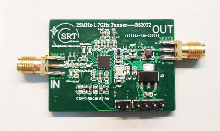
Tuner Design Example
In this example, we use R820T2 tuner on RTL-SDR dongles. This tuner PCB design uses the ultra-low noise linear power chip TPS7A4701. This chip supports wide voltage input, the input voltage range is from +3V to +36V. The ripple cannot be seen with an oscilloscope, and the maximum output current can reach 1A, which is sufficient for the previously designed low-noise amplifier. This design also features programmable output voltage.
This design uses R820T as the main component, the chip has built-in low-noise amplifier, mixer, automatic gain, phase-locked loop and so on. Using this chip, the radio frequency signal of 25MHz-1700MHz can be down-converted to an intermediate frequency of 3.57MHz. It is convenient to use low sample rate analog-to-digital converters to acquire RF signals.
This design uses R820T as the main component, the chip has built-in low-noise amplifier, mixer, automatic gain, phase-locked loop and so on. Using this chip, the radio frequency signal of 25MHz-1700MHz can be down-converted to an intermediate frequency of 3.57MHz. It is convenient to use low sample rate analog-to-digital converters to acquire RF signals.


MM3 Tuner Reviews
The MM3 Tuner is one of the most popular tuners on the market, and it has received a lot of positive reviews from customers. Many customers have reported that the MM3 Tuner has drastically improved the performance of their vehicles. They have also reported that it is easy to install and use.
The MM3 Tuner also has a lot of features that make it stand out from other tuners on the market. The built-in diagnostic system makes it easy to troubleshoot any issues with your engine, and the pre-programmed settings make it easy to get the most out of your engine.
Conclusion
So if you’re looking to get the most out of your vehicle, the MM3 Tuner is the way to go. With the MM3 Tuner, you can adjust the settings of your engine for peak performance and make your vehicle run as efficiently as possible.