Printed circuit boards (PCBs) are essential components of electronic devices, connecting all the parts together and allowing power to flow through the system. Despite their critical role, troubleshooting and resolving PCB problems can be a challenge. Fortunately, there are eight common PCB problems that are easy to diagnose and fix. By understanding the signs of these eight problems and the best solutions for each, you can quickly and efficiently identify and solve any PCB issues you may experience.
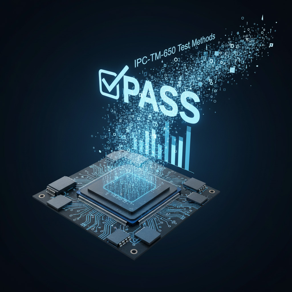
The 8 Most Common PCB Problems
When it comes to PCBs, there are eight common problems that you are likely to encounter. These issues can range from minor inconveniences to serious problems that can cause a device to malfunction. Knowing the signs and solutions to these problems is key to keeping your PCBs running smoothly.
Problem #1: Connection Issues
Connection issues on a PCB can range from minor annoyances to serious problems. Poor connections can prevent power from flowing correctly, resulting in erratic behavior or a complete lack of functionality. Other common signs of connection issues include intermittent power, flickering lights, surprising noises, and unexpected shutdowns.
Problem #2: Short Circuits
A short circuit occurs when two components on the board are connected in a manner that allows electricity to flow between them without passing through the intended components. This can cause a sudden surge of electricity that can damage components and, in some cases, even cause a fire.
Common signs of a short circuit include excessive heat, smoke, and sparks coming from the board. If you suspect that a short circuit is the cause of your PCB problems, it is important to turn off the device immediately and unplug it from the power source.
Problem #3: Insufficient Grounding
Grounding is an important safety feature that helps protect components and users from electrical shocks. Insufficient grounding can lead to unexpected behavior, such as a device suddenly turning on or off. It can also cause electrical shocks if a user touches two components on the board that is not properly grounded.
The most common signs of insufficient grounding are flickering lights, buzzing noises, and unexpected power surges. If you suspect that inadequate grounding is the cause of your PCB issues, it is important to check the wiring and make sure that all components are properly grounded.
Problem #4: Electrostatic Discharge Damage
Electrostatic discharge (ESD) is the sudden flow of electricity between two objects. This can cause serious damage to components on a PCB, resulting in erratic behavior or a complete lack of functionality. Common signs of ESD damage include intermittent power, flickering lights, and unexpected shutdowns.
To prevent ESD damage, it is important to always wear an anti-static wrist strap when handling components or working on the board. Additionally, it is important to avoid touching any of the components directly with your hands.
Problem #5: Component Damage
Components on a PCB can be damaged for a variety of reasons, including excessive heat, voltage spikes, and improper handling. Common signs of component damage include flickering lights, buzzing noises, and unexpected shutdowns.
If you suspect that a component on your board is damaged, it is important to identify the faulty component and replace it with a new one. Additionally, it is important to ensure that components are properly insulated and stored in appropriate conditions.
Problem #6: Excessive Heat
Excessive heat can cause components on a PCB to malfunction or fail. This can result in unexpected behavior, such as a device suddenly turning on or off. Common signs of excessive heat include flickering lights, buzzing noises, and unexpected shutdowns.
To prevent excessive heat from damaging your PCB, it is important to make sure that the board is properly ventilated and that all components are installed correctly. Additionally, it is important to use heat sinks or fans to help dissipate heat from components that generate a lot of heat.
Problem #7: Poorly Designed PCBs
Poorly designed PCBs can cause a wide range of problems, from intermittent power to unexpected shutdowns. Additionally, poorly designed PCBs can be difficult to troubleshoot, as it can be difficult to identify the source of the issue.
Common signs of a poorly designed PCB include intermittent power, flickering lights, and unexpected shutdowns. If you suspect that your PCB is poorly designed, it is important to review the design and make sure that all components are connected correctly. Additionally, it is important to double-check the power sources and make sure that they are providing the correct voltage.
Problem #8: Poor Quality Components
Poor quality components can cause a wide range of issues, from intermittent power to unexpected shutdowns. Common signs of poor-quality components include flickering lights, buzzing noises, and unexpected shutdowns.
To prevent issues caused by poor-quality components, it is important to only use components that meet the manufacturer’s specifications. Additionally, it is important to check the components for any signs of damage before installing them on the board.
What Cause PCB problems?
There are many common reasons why your PCB doesn’t work well. Some of these reasons can be easily fixed, while some others might require a re-design.
Too Many or Too Few Solder Pads
If you’ve ordered PCBs for your project, you may find that you have too many or too few solder pads. It’s important to know what amount of pads to order for your PCBs, but you also have to be aware of your design.
- If you have too many pads, it can create a few major issues.
- If your board has too many pads, there is a good chance that some of the pads will be bridged together.
- If the pads are bridged together, it can create a short circuit, which can cause your whole circuit to fail. Another issue that can happen if you have too many pads is that the pads can come in contact with one another.
- If the pads come in contact with each other, they can cause a short circuit.
The solution to having too many pads is to use a Dremel tool to remove some of the pads.
Incorrect Bending of Copper Tracks
Sometimes, the copper tracks on your PCBs don’t bend correctly. This can happen for a few reasons. First of all, you may have bent the tracks during the inspection. It can be easy to bend the tracks without realizing it, especially if you’re working with a high-volume PCB. You may also have bent the tracks during the manufacturing process. If that happens, the manufacturer can usually fix the issue by re-bending the tracks. The last way that the copper tracks can be bent incorrectly is during the design process. If you bend the tracks incorrectly, they can’t be fixed later on. The only solution is to create another PCB.
Lack of Adhesion During Soldering
Soldering pads are used to connect components to the PCB. If you’re working with a printed circuit board, you’ll find that most pads only have a small amount of solder on them. This is because you want to make sure that the pads don’t get too hot. If the pads get too hot, they can melt the PCB. If you’re having a problem where the pads aren’t sticking to the PCB, there are a few reasons why.
First of all, the pads could be too dry. If the pads are too dry, you can try adding a little bit of flux to them. Another reason why the pads may not be sticking is that you have too much solder on them. If the pads have too much solder on them, it can cause them not to adhere to the PCB.
Excessive Amount of Solder
Too much solder can be a problem, but it can also happen by accident. If you’re having issues with too much solder, it’s important to note that you don’t need to re-solder the entire pad. You can simply remove some of the solders to lower the amount. If you try to fix this issue by adding more solder, you’ll just create another problem. The pad may be too small for the amount of solder that you’re adding.
If that’s the case, the solder will start leaking out the side of the pad. Another issue that can happen if you have too much solder on the pad is that the excess solder can create a ball. The ball of solder can come between the pad and the component that you’re trying to solder.
Incorrectly Placed Components
If you’re having issues with a few components on your PCB, it could be that you’ve incorrectly placed the components. Most components are tiny and easy to misplace. If this happens to you, there may be a couple of ways that you can fix the issue. First of all, you can re-solder the component to the PCB. If the component is larger, you can sometimes use tweezers to move the component to the right place. It’s important to note that you should only do this if the component isn’t soldered to the PCB. In some cases, it may be easier to just replace the component with a correctly placed one.
Uneven Surface Mounting
The pads on a PCB are used to connect components and conduct electricity. Surface mount pads are used to connect small components like resistors or capacitors. If you have uneven surface mounting, it’s usually because the pads aren’t being soldered correctly. Sometimes, uneven surface mounting can also be caused by dirty pads. If the pads aren’t being soldered correctly, you can try cleaning the pads to see if that helps. You can also try using a different solder to see if that makes a difference.
Unmarked Track Areas
Sometimes, you’ll have an unmarked track area. A tracking area is an area on a PCB that isn’t used for components. An unmarked track area can happen for a few reasons. First of all, if you’re working with a high-volume PCB, it can happen if the PCB was used before. It can also happen if you’re using a partial PCB. It’s important to know that it’s okay to have unmarked track areas. It’s not a major issue. It’s a good thing. Unmarked track areas are useful for adding jumpers or making changes to the PCB.
Mistakes During Soldering And Manufacturing
There are a few mistakes that can happen during the soldering and manufacturing process. If you’re having issues with the pads on your PCBs, it may be because the holes are too small for the soldering iron. It can also be caused by the iron being too big. If the iron is too big, it will make it harder to control the iron. It can also cause extra damage to the PCB.
Another issue that can happen during soldering is that the iron may be too hot. If the iron is too hot, it can damage the PCB and the components on it. It can also cause the solder to flow too quickly, making it hard to control the iron. It’s important to note that all PCB manufacturers have standards for what temperatures are safe for soldering.
Excessive Solder Mask Dripping
During the manufacturing process, it is essential to have the right amount of solder mask applied. If there is too much of the protective coating on the PCB, it can cause problems with the electrical connection. If the solder mask is applied too thick, it can create an excessive amount of droplets on the PCB, causing electrical issues and decreasing the quality of the product. To prevent this issue, manufacturers should be sure to purchase the right amount of solder mask for each job.
Too Many Via Holes
The holes on a printed circuit board can be used for a number of things, from installing input/output ports to housing electrical components. While there are a number of ways to install these holes on the board, you want to avoid placing more than one via per hole. Placing one via per hole is the standard.
If you have a layout that requires you to use more than one via per hole, you need to review your design to make sure it is not something that can be fixed. This can cause a number of issues, such as electrical shorts. You also want to ensure that the distance between each via is no less than 1 cm. If you have a layout that requires you to use more than one via per hole, you need to review your design to make sure it is not something that can be fixed.
How to identify the issues on PCB?
Identifying the source of an issue on a printed circuit board (PCB) requires systematic approach. The process of diagnosis involves careful examination of the board and its components to identify any potential faults. These are the common methods:
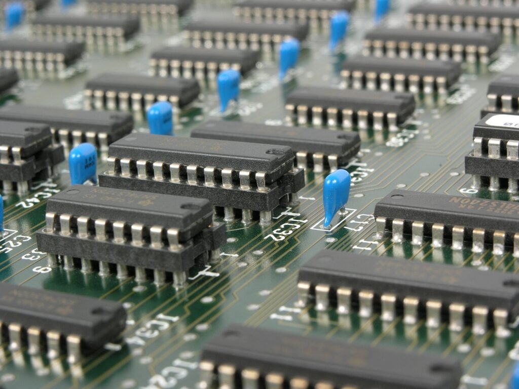
Visual inspection
This is a simple but effective way to identify any obvious physical damage or debris on the PCB. Visual inspection involves examining the components, printed circuit traces, solder joints, and other physical characteristics of the PCB for defects. This process is typically done prior to manufacturing, during assembly, and after final testing.
The visual inspection can detect the abnormalities includes:
- incorrect component placement
- poor soldering
- missing components
- incorrect trace routing
Visual inspection is most often conducted manually, but automated inspection systems are gaining popularity as they are faster and more reliable than manual visual inspection. Automated inspection systems use cameras, sensors, and other imaging techniques to detect defects in the board.
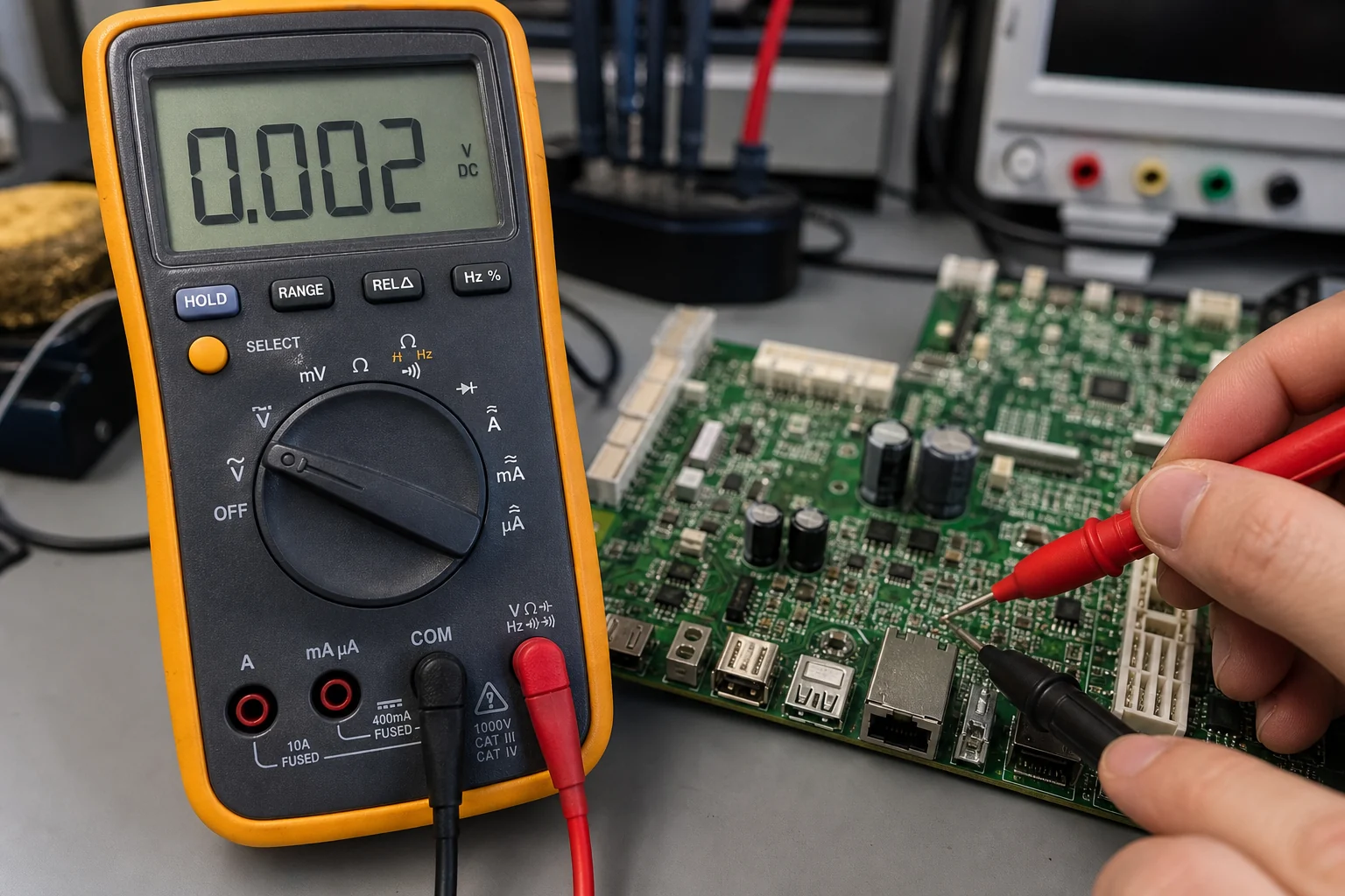
Power Supply Testing
Power supply testing for printed circuit boards (PCBs) is a critical part of the design and manufacturing process. Proper power supply testing ensures that the PCB will be able to meet its intended functionality and performance goals. Power supply testing should be conducted in several stages, for example:
- voltage testing
- current testing
- resistance testing
- noise testing
- ripple testing
- transient response testing
- dynamic load testing
Each test should be conducted in accordance with the manufacturer’s specifications and safety standards. You can use an oscilloscope, multimeter or an ohmmeter to do these operations.
Electrical Continuity Testing
This type of testing is used to check for open or short circuits in the conductive paths between components on the board. It is typically done either before or after the soldering process to detect any potential issues with the electrical connections. The most common method of electrical continuity testing includes:
- electrical resistance testing
- current leakage tests
- voltage drop tests
- insulation resistance tests
The electrical continuity testing can be done manually or using automated test equipment. Manual testing involves connecting a test probe to each of the conductive paths on the board, and then checking for continuity. Automated testing uses specialized test equipment to run tests on the entire board in a single operation. This can save time and money when testing large numbers of PCBs.
Component Testing
component testing is typically done either with a manual or automated process. In the manual process, the components on the board are tested using a combination of visual inspection and continuity testing. The automated process uses specialized test equipment such as in-circuit testers and flying-probe testers. these tests can also detect any issues that may have occurred during the manufacturing process:
- incorrect solder joint connections
- improper component placement
- opens or short circuit
Both manual and automated testing should be done prior to assembly, during assembly, and after assembly. This will help ensure that the board is functioning correctly before it is shipped to the customer.
Signal Testing
PCB signal testing is a process used to measure the electrical signals that are being sent through a printed circuit board. The main purpose of PCB signal testing is to ensure that the printed circuit board is functioning properly and efficiently. The testing involves several steps, includes:
- crosstalk between the different signal traces
- impedance, capacitance, and inductance
- signal integrity analysis of the various components
- electromagnetic interference on circuit
The specific equipment used for PCB signal testing may depend on the type of PCB being tested, as well as the requirements of the application. Generally, this testing is accomplished with an oscilloscope, logic analyzer, spectrum analyzer, or other specialized testing equipment.
Solutions to Common PCB Problems
Once you have identified the cause of the issue, you can begin to troubleshoot and resolve the problem. Generally speaking, the best solution for each problem will depend on the root cause. However, some general solutions can be applied to many common PCB issues.
The first step to resolving any PCB issue is to identify the cause. This can be done by carefully inspecting the board and looking for any signs of damage or malfunctioning components. Additionally, it is important to review the design of the PCB and make sure that all components are connected properly.
Once the cause has been identified, the next step is to determine the best solution for the problem. In some cases, this may involve replacing components or rewiring the board. In other cases, the problem may be resolved by simply adding additional insulation or heat sinks to the board.
It is also important to make sure that the board is properly ventilated and that all components are installed correctly. Additionally, it is important to check the power sources and make sure that they are providing the correct voltage.
Finally, it is important to ensure that all components are of the highest quality and that they meet the manufacturer’s specifications. This can help to prevent issues caused by poor-quality components and ensure that the board operates correctly.
Conclusion
PCB problems can be a challenge to diagnose and fix, but understanding the eight most common issues and their respective solutions can help make the process easier. By being aware of the signs of these eight problems and the best solutions for each, you can quickly and efficiently identify and resolve any PCB issues you may experience.