The ESP32-WROOM dev board is a versatile, dual-core IoT development platform with integrated Wi-Fi and Bluetooth, featuring 30+ GPIO pins for the wide range of peripherals. We’ll introduce its key features, pin configurations, schematic insights.
Features of ESP32-WROOM
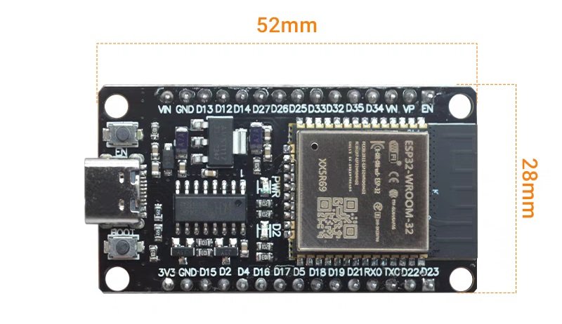
- Dual-core 240MHz CPU for fast multitasking.
- Built-in Wi-Fi + Bluetooth for wireless connectivity.
- Capacitive touch, Hall sensor, SD card, and high-speed interfaces.
- Low-power sleep modes to extend battery life.
- 5V USB-powered (on-board 3.3V regulator) with 3.0–3.6V operation.
- Wide temp range (-40°C to 85°C) for harsh environments.
ESP32-WROOM Pins
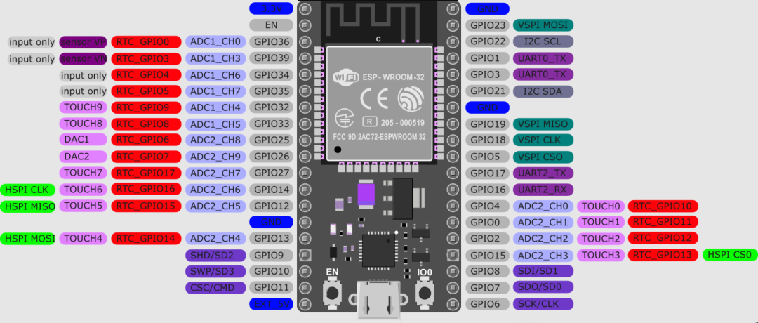
Digital I/O Pins (GPIO0-GPIO31)
General Purpose Input/Output
Most pins (e.g., GPIO4, GPIO5, GPIO12-GPIO23) function as digital inputs or outputs. These support pull-up/pull-down resistors and can be configured for interrupts.
Special Considerations for Boot Behavior
- GPIO0: Pulled low to enter download mode; outputs PWM by default at boot.
- GPIO15: Pulled low during boot; avoid the pull-up resistor for stable startup.
Analog Pins (ADC and DAC Channels)
Analog-to-Digital Conversion (ADC)
- ADC1 (Channels 0-7): Mapped to GPIOs 36-39, 32-35 (e.g., GPIO36 for voltage sensing).
- ADC2 (Channels 0-9): GPIOs 4, 0, 2, 15, 13, 12, 14, 27, 25, 26. Note: ADC2 is disabled when Wi-Fi is active.
Usage Tip: Calibrate ADC readings for non-linear behavior, especially near 0V and 3.3V.
Digital-to-Analog Conversion (DAC)
- DAC1: GPIO25
- DAC2: GPIO26
UsedacWrite()to generate analog voltages (0-255 range), suitable for PWM-like applications.
Special Function Pins
Capacitive Touch Sensors
10 GPIOs (e.g., GPIO4, GPIO0, GPIO2, GPIO15) support capacitive touch input, detecting finger proximity via charge changes.
Application: Replace mechanical buttons with touch-sensitive pads for sleek interfaces.
RTC GPIOs for Low-Power Modes
Pins like GPIO36, GPIO39, and GPIO4 can wake the board from deep sleep when triggered, essential for battery-powered devices.
Configuration: Enable RTC functionality in the ESP-IDF framework to utilize these pins.
Communication Interfaces
- I2C: Default pins SDA (GPIO21), SCL (GPIO22); configurable for other GPIOs.
- SPI: MOSI (GPIO23), MISO (GPIO19), CLK (GPIO18), SS (GPIO5/15), supporting high-speed data transfer.
- UART: TX/RX pins (e.g., GPIO1/TX, GPIO3/RX) for serial communication with peripherals.
ESP32-WROOM Schematic
The schematic of ESP32-WROOM dev board includes these hardware architecture or key components:
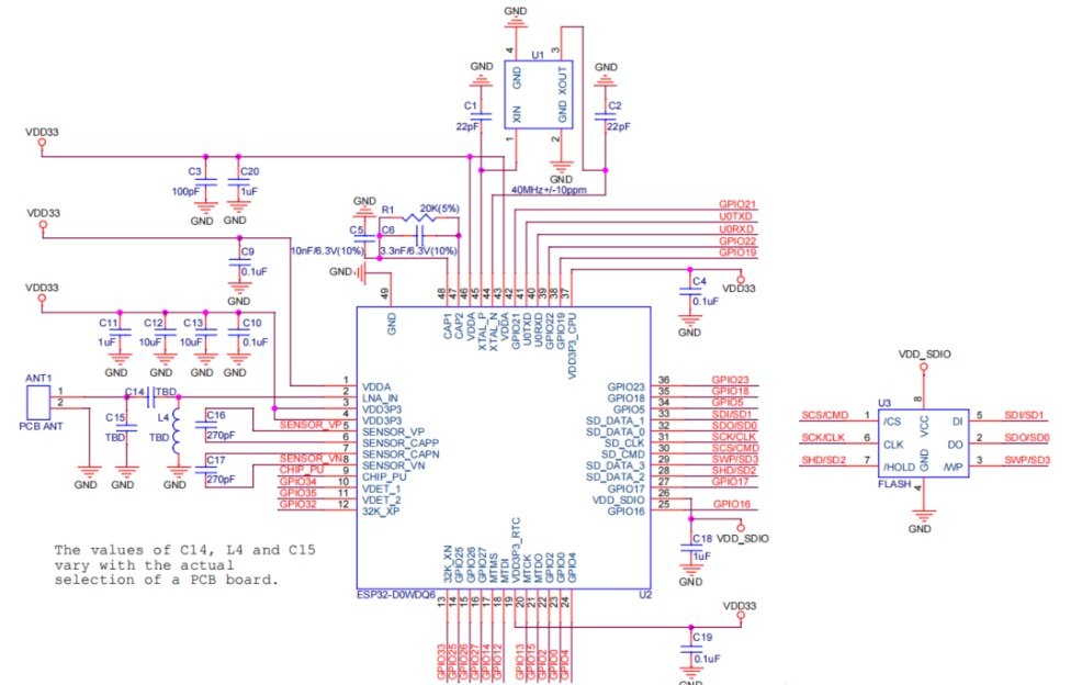
1. Clock Circuit (U1: 40MHz Crystal)
- The 40MHz crystal (XTAL_N, XTAL_P pins) provides the primary clock source for the ESP32 chip (U2), ensuring stable operation. Capacitors (C1, C2) stabilize the oscillator, critical for timing-sensitive peripherals like Wi-Fi and Bluetooth.
2. Power Management
- VDD33 (3.3V power rail) is filtered by multiple capacitors (e.g., C3, C20, C19) to reduce noise, ensuring clean power for the ESP32, flash memory (U3), and external peripherals. This filtering is vital for analog signals (e.g., ADC inputs) to avoid interference.
3. Flash Memory (U3: SDIO Interface)
- The ESP32 communicates with the external flash (e.g., SPI flash via SDIO) using pins:
- GPIO26 (SD_DATA0), GPIO27 (SD_DATA1), GPIO28 (SD_DATA2), GPIO29 (SD_DATA3) (data lines),
- GPIO30 (SD_CMD) (command line),
- GPIO31 (SD_CLK) (clock line).
These pins (part of the SPI/SDIO peripheral) store firmware and user data, enabling the board to boot and run applications.
4. Antenna and RF Circuitry (ANT1)
- The PCB antenna (ANT1) connects to the ESP32’s RF pins (e.g., LNA_IN, VDD_SP, VDD_RF), supporting Wi-Fi (2.4GHz) and Bluetooth communication. Components like L4 (inductor) and C14/C15 (tuning capacitors) optimize RF performance, though their values vary by PCB design (as noted in the schematic).
5. GPIO and Peripheral Connections
- Sensor Interface: Pins like SENSOR_VP (GPIO36) and SENSOR_VN (GPIO39) (ADC1 channels) are routed for analog sensor inputs (e.g., voltage/current sensing), leveraging the ESP32’s 12-bit ADC.
- Capacitive Touch Pins: GPIO0, GPIO2, etc. (marked as SENSOR_CAP_P/N) support touch-sensitive applications, integrated with the ESP32’s capacitive touch controller.
- Debug and Boot Pins: GPIO0 (download mode trigger) and GPIO15 (boot configuration) are visible, with pull-up/pull-down resistors (e.g., R1 for GPIO0) ensuring correct startup behavior.
6. Filtering and Decoupling
- Decoupling capacitors (e.g., 0.1μF, 1μF) near power pins (VDD33, GND) minimize voltage fluctuations, while RF-specific components (e.g., TBC0, TBC1 balun for antenna) optimize wireless signal integrity.
Conclusion
That’s all about the ESP32 wroom dev board, maybe we’ll add some related practical application or project for study later. Anywell, if you have any question, feel free to contact us for help!

