In this article, I will discuss the benefits of Schottky diodes, their applications, and what makes them different from other diodes.
Introduction to Anti-Reverse Flow Schottky Diode
An anti-reverse flow Schottky diode is a type of semiconductor device that serves as a one-way valve for electrical current. It is designed to prevent current from flowing in the opposite direction, which could cause damage to the circuit or device. The Schottky diode is named after Walter H. Schottky, who invented it in 1938.
The anti-reverse flow Schottky diode is commonly used in electronic devices such as power supplies, battery chargers, and solar panels. It is particularly useful in circuits where there is a risk of reverse current flow due to the nature of the load or the power source. For example, in a solar panel system, the diode can prevent the battery from discharging through the solar cells at night.
Overall, the anti-reverse flow Schottky diode is an essential component in many electronic systems to ensure proper and safe operation.

Understanding the Schottky Diode Forward Voltage
The forward voltage drop of a Schottky diode is typically between 0.15 to 0.45 volts, which is much lower than the 0.6 to 0.7 volts for a regular diode. This low forward voltage drop means that Schottky diodes are more efficient in converting electrical energy into light or heat. Moreover, this low forward voltage drop also makes them ideal for low voltage applications.
How does the Schottky Diode Work?
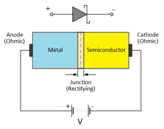
A Schottky diode works by creating a barrier between a metal and a semiconductor. The metal region is the positive electrode, and the N-type semiconductor region is the negative electrode. Since there are many electrons in the semiconductor and only a few in the metal, the electrons diffuse from the semiconductor to the metal. This creates a potential barrier that blocks current flow in the reverse direction. When the electron drift movement and diffusion movement reach a balance, a Schottky barrier is formed.

A typical Schottky rectifier uses an N-type semiconductor substrate with an N-epitaxial layer doped with arsenic. Molybdenum or aluminum is used to make the barrier layer for the anode, and silicon dioxide is used to improve the withstand voltage value of the tube. An N+ cathode layer is formed under the substrate to reduce the contact resistance of the cathode. By adjusting the structural parameters, a Schottky barrier is formed between the N-type substrate and the anode metal. Applying a forward bias to both ends of the Schottky barrier makes the barrier layer narrower and its resistance smaller, while a reverse bias widens the barrier layer and increases its resistance.
Structure of Schottky Diode
The new high-voltage SBD differs from traditional SBD in both structure and material. Traditional SBDs use metal-semiconductor contacts with metals like aluminum, gold, molybdenum, nickel, or titanium and semiconductors such as silicon (Si) or gallium arsenide (GaAs).
To achieve good frequency characteristics, N-type semiconductor materials are chosen for the substrate due to the higher mobility of electrons than holes. A high-resistance N- thin layer is also epitaxial on the N+ substrate to reduce junction capacitance and increase reverse breakdown voltage without increasing series resistance too much.
When a metal comes into contact with a semiconductor, electrons diffuse from the semiconductor to the metal due to the Fermi level of the metal being lower than that of the semiconductor. This results in the metal becoming negatively charged and the semiconductor becoming positively charged. Since metals are perfect conductors, the negative charges are distributed only within a thin atomic-sized layer on the surface.

N-type semiconductors have positively charged donor impurity atoms that are distributed over a larger area. When electrons diffuse from the semiconductor to the metal, a depletion layer, a self-built electric field, and a potential barrier are formed, which only exists on the N-type semiconductor side. The self-built electric field in the barrier region points from the N-type region to the metal. As the thermal electron emission self-built field increases, the drift current opposite to the diffusion current increases until it reaches a dynamic equilibrium, forming a contact potential between the metal and the semiconductor, known as the Schottky barrier.
When the voltage is zero, the diffusion current of electrons equals the reverse drift current, resulting in a dynamic equilibrium. Applying a forward bias weakens the self-built field and reduces the potential barrier on the semiconductor side, allowing a forward current to flow from the metal to the semiconductor. On the other hand, applying a reverse bias enhances the self-built field and increases the height of the potential barrier, causing a small reverse current to flow from the semiconductor to the metal. Thus, like a PN junction diode, the SBD is a nonlinear device that conducts unidirectionally.
Applications of Schottky Diode in Modern Electronics
Schottky diodes have a wide range of applications in modern electronics. One of the most common applications is in power rectification, where they are used to convert AC power to DC power. They can also be used in voltage clamping, where they limit the maximum voltage in a circuit. Additionally, Schottky diodes are widely used in high-frequency applications, such as in radio frequency detectors and mixers.
Advantages and Disadvantages of Schottky Diode
Advantages of Schottky Diode:
- Low forward voltage drop compared to other diodes, which results in less power loss and higher efficiency.
- Faster switching speed than other diodes due to lower junction capacitance, which makes it ideal for high-frequency applications.
- Lower reverse recovery time than other diodes, which reduces the risk of damage from reverse voltage spikes.
- Higher operating temperature range than other diodes, which makes it suitable for use in high-temperature environments.
- Can be used as a rectifier in power supplies, voltage clamping, signal demodulation, and other applications.
Disadvantages of Schottky Diode:
- Lower reverse breakdown voltage compared to other diodes, which limits its use in high-voltage applications.
- Higher leakage current than other diodes, which can cause issues in circuits that require low power consumption.
- More susceptible to thermal runaway due to its lower forward voltage drop, which can cause damage to the diode and the surrounding components.
- Sensitive to electrostatic discharge (ESD), which can cause permanent damage to the diode.
- Limited availability of high-voltage Schottky diodes compared to other types of diodes.
Example:
An example of a Schottky diode is the 1N5817. It has a forward voltage drop of 0.45V and a maximum forward current of 1A. It can be used for rectification, voltage clamping, and other applications in low-voltage circuits. However, it may not be suitable for high-voltage applications due to its lower reverse breakdown voltage.
Schottky Diode vs. Regular Diode
The main difference between a Schottky diode and a regular diode is the type of junction used. Regular diodes use a P-N junction, while Schottky diodes use a metal-semiconductor junction. This difference in junction type results in a lower forward voltage drop for Schottky diodes, as well as a faster switching speed and lower reverse recovery time.
Choosing the Right Schottky Diode for Your Application
When choosing a Schottky diode for your application, there are several factors to consider. The first factor is the forward voltage drop, which determines the minimum voltage at which the diode will conduct.
The second factor is the reverse voltage rating, which determines the maximum voltage that the diode can withstand in the reverse direction.
Finally, the third factor is the maximum current rating, which determines the maximum current that the diode can handle.


