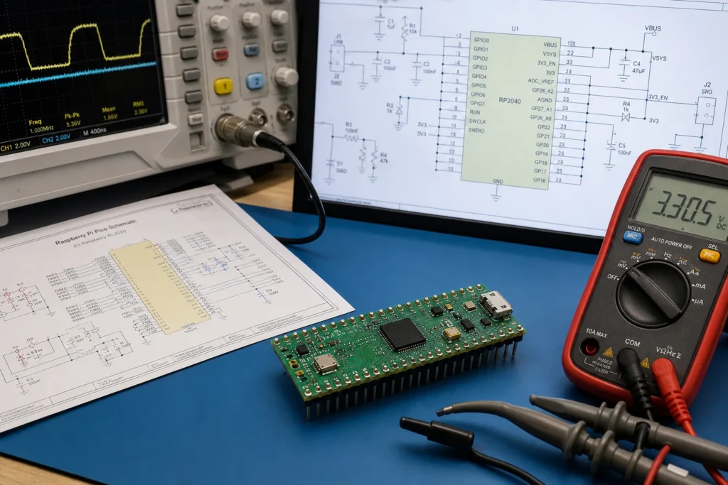
When a Raspberry Pi Pico board powers up but USB does not enumerate, the ADC reads garbage, or SWD never connects, the problem is often visible in the schematic before the first board is assembled. A Pi Pico schematic is not just a drawing of the RP2040 and some headers. It is the map for power sequencing, flash boot, USB behavior, debug access, and the quiet analog details that determine whether bring-up takes an hour or a week.
This guide explains how to read a Pi Pico schematic with a board-level mindset. The goal is not to repeat the pinout. It is to show what deserves attention before you copy the reference design, spin a custom carrier, or debug a board that looks correct at first glance.
Before You Start with a Pi Pico Schematic Review
Keep three references open at the same time: the official Pico board schematic, the RP2040 hardware design guidance, and your own netlist or custom board draft. If you only compare pin names, you will miss the real failure points. The useful review is about rails, resets, flash access, USB routing, and whether test access still exists once the board is assembled.
What a Pi Pico Schematic Should Tell You Before First Power-Up
A good Pi Pico schematic answers four questions immediately: where the board gets power, how the RP2040 boots, how firmware will be loaded or debugged, and which signals are safe to break out without collateral problems. If the sheet makes those answers hard to see, the board will be harder to validate later.
That is why a schematic review should start with system behavior rather than peripheral wish lists. The GPIO count matters later. During bring-up, the first pass is more basic: can the regulator start cleanly, can the flash talk to the MCU, can the USB path survive routing and ESD choices, and can a technician still probe the important nets?
Start with the Power Path Instead of the GPIO Labels
On the Pico board, VBUS feeds VSYS through a diode, and VSYS then feeds the on-board 3.3 V regulator. That sounds simple, but it creates several review checkpoints. If your custom board changes the OR-ing strategy, the regulator, or the input source, you need to decide what should happen when USB is connected at the same time as an external supply. A board that works on the bench but back-feeds a host port or drops out during hot-plug is not really validated.
Check the rails that quietly decide bring-up
Look at VBUS, VSYS, 3V3, and 3V3_EN first. Confirm the intended input range, the regulator topology, and the shutdown behavior. The Pico family documentation notes that VSYS is the main input rail and that the board uses a buck-boost style 3.3 V supply. That is useful in practice because a copied reference design behaves differently from a board that swaps in a cheaper LDO with less margin under USB load, sensor bursts, or cable loss.
Then check whether ADC_AVDD is treated as a real analog supply node or as an afterthought. Even if your application does not need precision analog work, sloppy decoupling and long return paths make debug harder because bad power can masquerade as firmware or USB trouble. On low-cost prototypes, this is one of the easiest places to save two parts on paper and lose days in measurement time.
One more practical detail matters on the official Pico board: GPIO29 can monitor the board supply through a divider to ADC3. That can be useful for battery or rail checks, but only if you remember the divider and the board-level implementation. Engineers sometimes trust the raw ADC reading and diagnose a power issue that does not exist.
USB and Boot Circuitry Usually Break Before the Code Does
If a Pi Pico schematic is being reviewed for a custom board, the USB section deserves the same attention as the MCU itself. The common failure pattern is not a dramatic short. It is a board that powers, exposes a COM port inconsistently, or enters a boot state only when the cable or host changes. Those are schematic-level problems as much as layout problems.
Review the USB connector path, protection parts, D+ and D- continuity, and any added series resistors or common-mode filtering. Make sure those choices still match the intended cable length, ESD environment, and assembly process. A protection part placed for convenience rather than signal entry can satisfy a checklist while still leaving the real discharge path messy.
Boot behavior is the next checkpoint. The Pico reference design depends on the external flash path being correct every time, not just after rework. If the QSPI flash rails, pull behavior, or line assignments are unclear on the schematic, the symptom may look like dead silicon when the real cause is a schematic decision that left no margin for solder voiding, skewed stencil release on a small package, or awkward probe access around the flash device.
GPIO, ADC, and Debug Nets Need a Real Use-Case Review
A pinout article tells you what each pin can do. A schematic review asks whether your chosen function still works once the board is powered, assembled, and enclosed. That is where many Pico-derived boards drift into avoidable trouble.
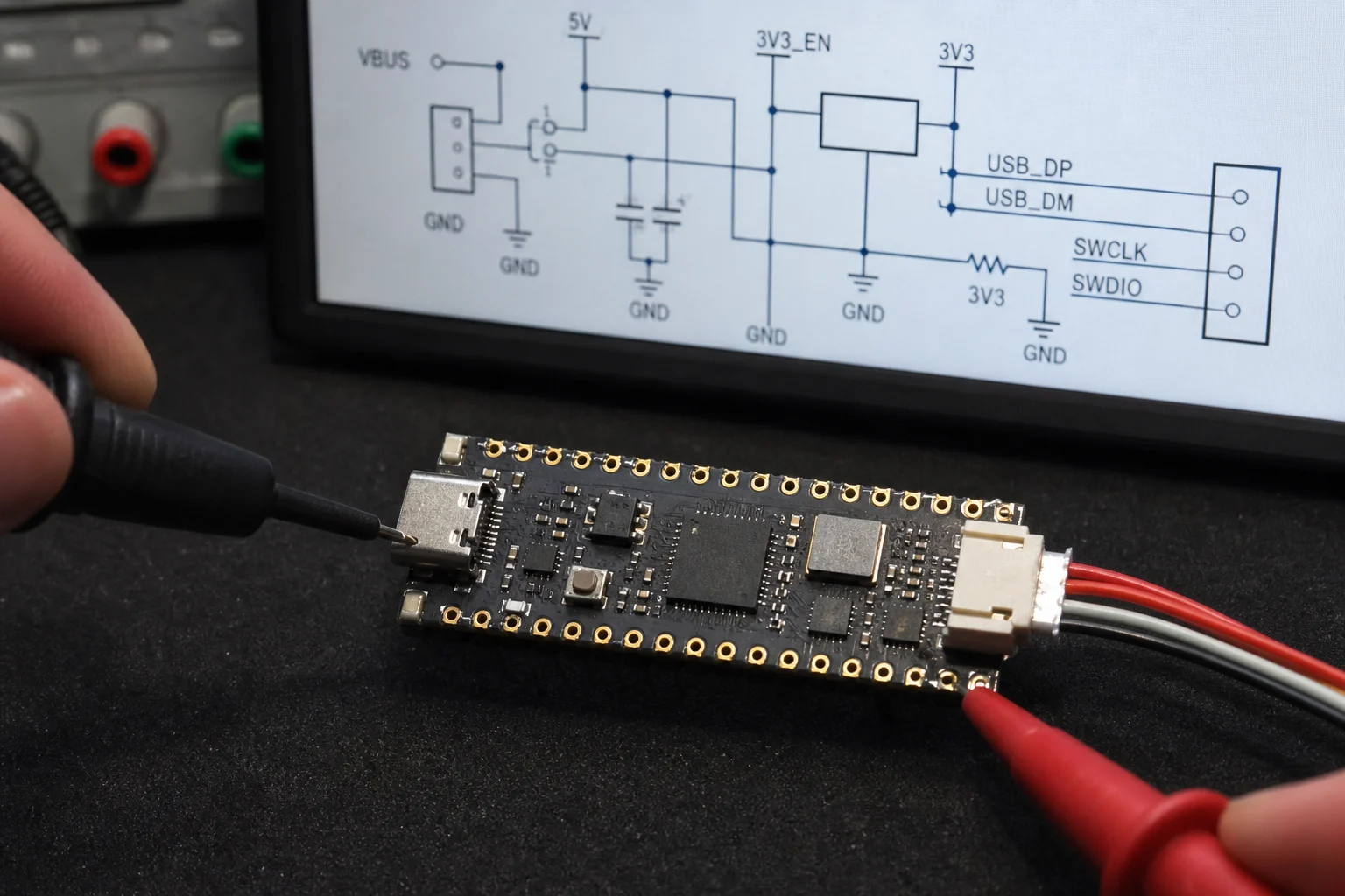
Start with the signals you will need when something goes wrong: RUN, SWD, UART debug, the boot path, and any rail-sense signals. If SWD pads are present but hidden under a module, or if the only reset access is a tiny pad next to a noisy converter, the schematic may be technically complete but operationally weak. The same logic applies to production test. If the first article build fails and there is nowhere to measure reset timing, flash activity, or rail quality, DFT was not really considered.
For analog and mixed-signal use, separate what must be quiet from what is merely functional. The RP2040 can tolerate a lot in hobby projects, but production boards are less forgiving. A noisy analog path, weak local decoupling, or casual sensor return routing can look acceptable in a diagram yet create unstable readings that only appear after enclosure grounding, cable changes, or temperature rise.
If you need a quick reference for pin capabilities while reviewing the sheet, the existing Pi Pico pinout guide is a useful companion. Use it to confirm function mapping, but keep the schematic review focused on rails, interfaces, and bring-up access rather than on header labels alone.
Why Copying the Reference Schematic Still Leaves Risk on a Custom Board
The official Raspberry Pi references are strong starting points, but they do not remove the need for engineering judgment. As soon as you change the regulator, connector orientation, flash package, board shape, sensor load, or enclosure constraints, you change the assumptions that made the original design robust.
A simple example is the power tree. The official Pico arrangement is designed around a known regulator path and board usage model. If your board must run from battery, share power with a motor driver, or survive industrial ESD events, the reference is no longer a drop-in answer. The same is true for debug headers. A connector that is fine on a development board may be the wrong choice on a service-limited field unit where pogo access or a keyed header reduces repair risk.
This is also where the broader RP2040 microcontroller breakdown helps. It covers the silicon and interface capability. Your schematic review should translate those capabilities into concrete decisions about power integrity, flash reliability, probe access, and what the assembly house must inspect before boards leave the line.
A Fast Review Checklist Before You Release the Board
Before sending a Pico-derived board to fabrication, run a short checklist that reflects real build and debug work:
- Power path is explicit from VBUS or external input to VSYS and 3.3 V, with no ambiguous back-feed behavior.
- ADC_AVDD, decoupling, and return paths are intentional, not copied blindly.
- QSPI flash rails and signal assignments are clear enough to troubleshoot without guessing.
- USB protection and connector choices match the actual cable, enclosure, and ESD environment.
- RUN, SWD, and at least one practical debug path remain accessible after assembly.
- Key test points can still be probed when the board is populated, not just when the PCB is bare.
- Any VSYS sensing or divider assumptions are documented so firmware and test engineers do not misread the numbers.
That list is short on purpose. If a board misses any one of those points, the cost usually shows up later as rework, uncertain root cause analysis, or avoidable NPI delay.
The Best Pi Pico Schematic Is the One You Can Debug Under Pressure
The Pi Pico schematic becomes valuable when it helps you answer the ugly questions quickly: why the board does not boot, why USB is unstable, why ADC behavior changed after enclosure integration, or why one build lot fails while another passes. That means the best schematic is not the prettiest one. It is the one that preserves power clarity, debug access, and manufacturing intent all the way from design review to first article inspection.
If you are reviewing a Pico board or building an RP2040 derivative, treat the schematic as a bring-up document, not just a documentation artifact. That shift alone prevents many of the slow, expensive failures that only appear after the board leaves the CAD screen.
FAQ
Is a Pi Pico pinout article enough if I need to review the schematic?
No. A pinout helps you identify functions, but a schematic review must also cover the power path, flash boot circuit, USB behavior, debug access, and measurement points. Those are the items that usually decide bring-up success.
What part of the Pi Pico schematic should I check first on a custom board?
Start with the power tree. Confirm how VBUS or the external source reaches VSYS, how 3.3 V is generated, and whether shutdown, ADC supply filtering, and rail monitoring still make sense for your board. If the power path is weak, later GPIO checks will not matter much.
Why can a copied RP2040 reference schematic still fail in production?
Because the reference assumes a specific regulator, board size, connector setup, and use case. Changing the flash package, power source, ESD strategy, or test access can introduce new risks even if the core MCU section looks familiar.
Which debug signals should stay accessible on a Pi Pico derived design?
At minimum, keep reliable access to RUN, SWD, power rails, and one practical interface for observing boot or firmware behavior. If those nets are inaccessible after assembly, root-cause work becomes slower and rework becomes more expensive.