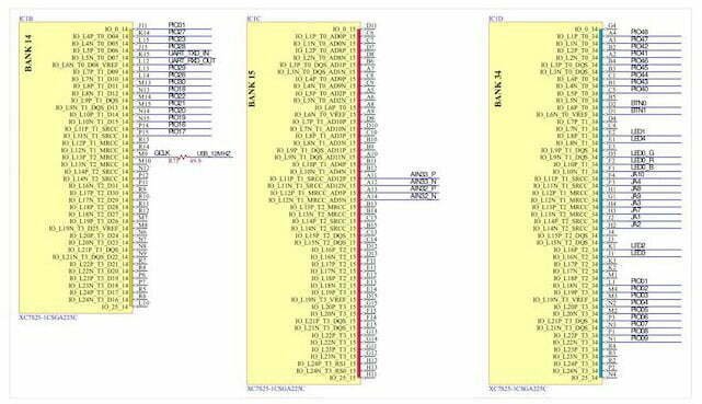
What is the schematic Symbol?
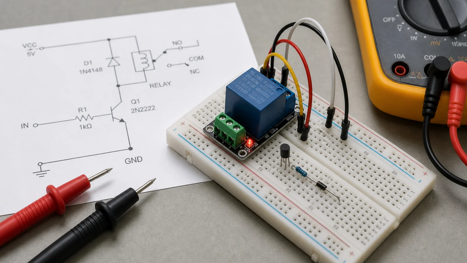
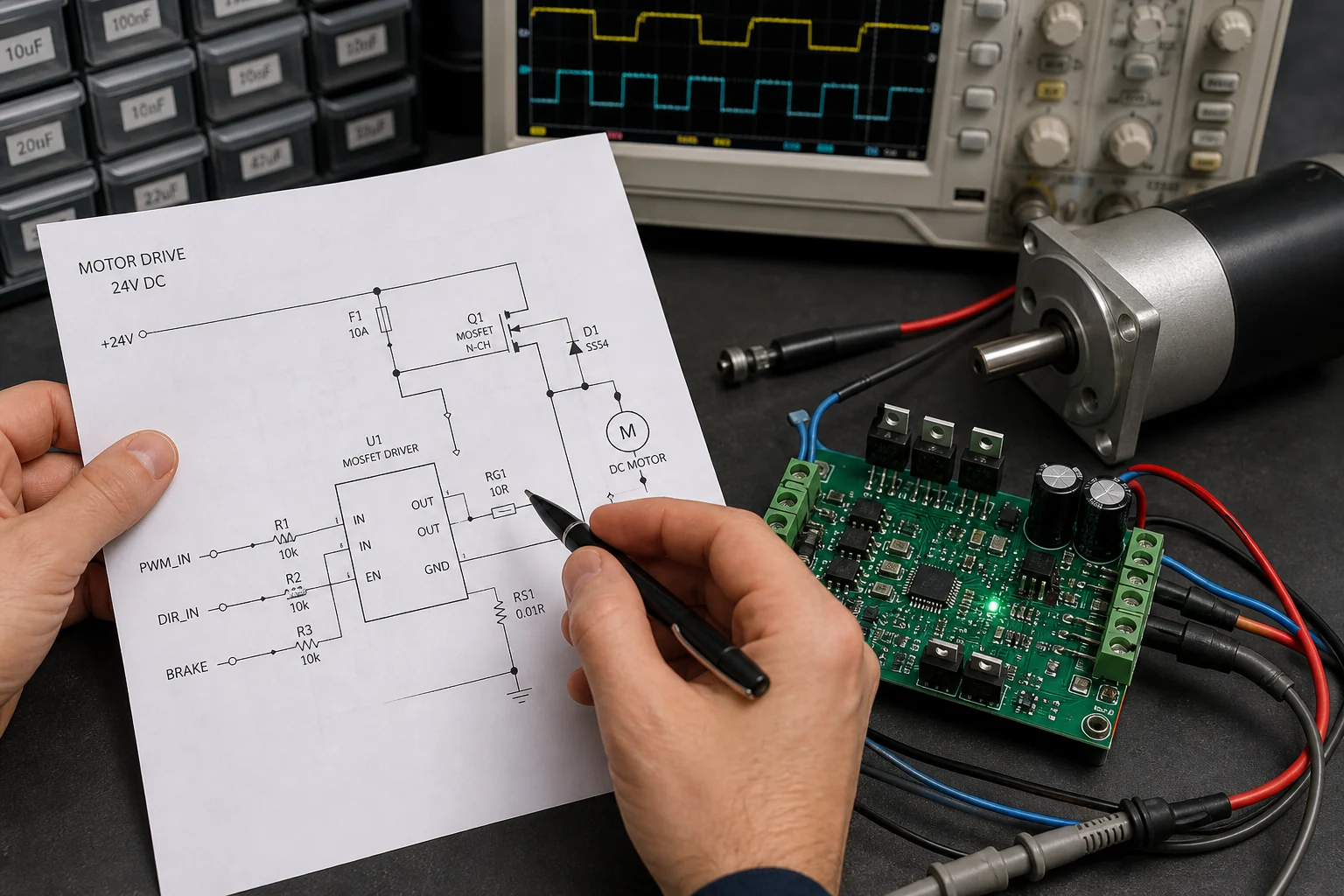
A schematic symbol is a graphical representation of an electrical or electronic component. There are many schematic symbols in schematic library. And the schematic library is one of the important steps in pcb reverse engineering.
Structure of Schematic Symbols
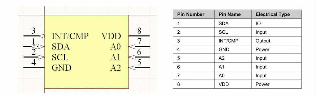
There are several essential elements that constitute a schematic symbol:
Profile – profile may be different depending on the nature of the component;
Pins – including names, numbers, input and output attributes, etc;
Component Labeling – Number, Model, Simple Description;
How to Create Schematic Symbols
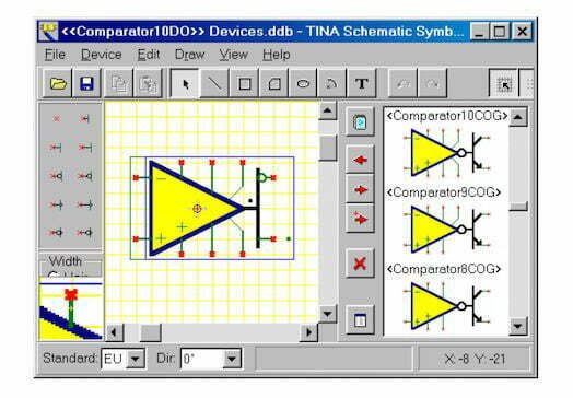
There are several ways you can choose from to build your own schematic symbol:
- Create from the pcb tool’s own library.
- Extract from existing schematic.
- Download from the original official website.
- Manual creation of device-based data sheets.
Create by Alitium designer
Each schematic symbol represents an actual electronic component. When drawing the schematic library, we do not need to draw the actual device, but only need to clearly express the electrical pin properties and connection relationships of the device.
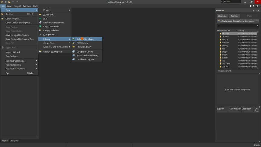
1. Open Schematic library
First, open Altium Designer software, first find the schematic library in File->New->Library, click Open.
2. Place Rectangle
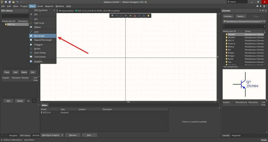
Then, select Place->Rectangle, and place a square to represent the shape of the chip. The size is determined by the chip, which can be placed first and the size can be changed later.
3. Place Pin and setting properties
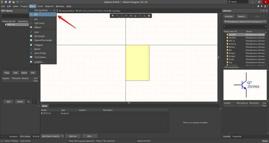
Next, open the data sheet of the chip and find the product pinout. Select Place->Pin, and place the pins of the chip in turn according to the pin map. It should be noted here that when placing the pin, the side with the rice size should face the outside of the chip. Because this side has electrical properties, it is used to connect wires or other components when drawing a schematic.
When the placement is complete, change the pin’s serial number, name, length and other properties in the property bar on the right.
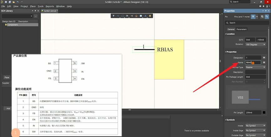
After changing the properties of pin No. 1, you can hold down the shift key of the keyboard, move the mouse to Pin No. 1, and press and hold the left mouse button to move to quickly generate the second pin, and then change the properties.
4. Rename Schematic Library
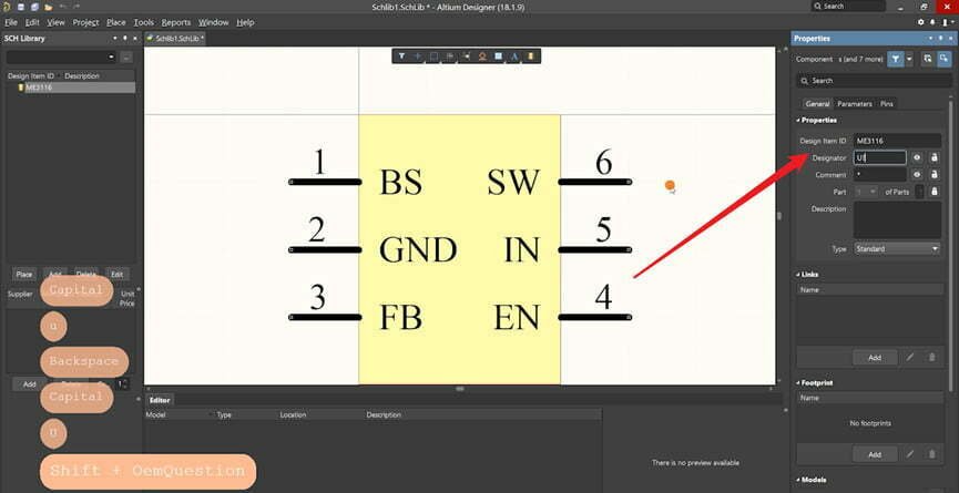
After drawing a component, rename the schematic library.
5. Save Files
The final step is to save the file to the computer. Be careful to distinguish the naming of the different schematic symbols to prevent confusion.
Creating Schematic Symbols that Preserve Pin Meaning and Netlist Accuracy
A schematic symbol is a data model for connectivity, review, and electrical rules, not merely a drawing that resembles the package. When adding a part to an express pcb component library or another CAD library, the governing source should be the exact manufacturer datasheet revision and complete ordering code. Pin numbers must map to the physical package, pin names must preserve active-low and polarity meaning, electrical types must support useful rule checks, and hidden or stacked pins must never conceal required connections. The symbol should remain readable at normal scale, separate logical functions clearly, link to the correct footprint and documentation, and pass an independent symbol-to-package comparison before project use.
- Datasheet and ordering-code anchor: record manufacturer, full part number, package drawing, pin table, revision, source link, and date in library metadata.
- Physical pin-number mapping: verify every number, letter, exposed pad, no-connect, duplicated supply, and package-specific omission against the drawing.
- Logical symbol organization: group power, analog, digital, configuration, bus, and control pins while preserving names, polarity marks, and alternate functions.
- Electrical-rule behavior: assign input, output, bidirectional, passive, power, open-drain, and no-connect types to catch real mistakes without noise.
- Library release validation: perform second-person review, footprint cross-probe, test schematic, netlist inspection, version control, and controlled replacement of older symbols.
Symbol vs Footprints
There are a couple key differences between symbols and footprints in electronic design. First, symbols are typically used to represent components in a schematic, while footprints are used to represent the physical dimensions of a component on a PCB. Second, symbols generally only include the electrical connections of a component, while footprints also include the physical dimensions and layout of the component on the PCB.
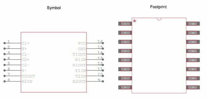
Footprints are generally more detailed than symbols, since they need to include the physical dimensions of the component. This means that creating a footprint can be more time-consuming than creating a symbol. However, having a accurate and well-designed footprint is essential for ensuring that your PCB is correctly manufactured.