In high-frequency and high-speed PCB design, choosing the right transmission line structure—stripline or microstrip—is pivotal for ensuring signal integrity, minimizing interference, and balancing cost-effectiveness. Both structures serve as fundamental building blocks for RF/microwave circuits and high-speed digital systems, but their distinct geometries and electromagnetic behaviors dictate their suitability for specific applications. This article dissects the core differences between stripline and microstrip, exploring their designs, electrical properties, and practical implications for PCB engineers.
What is Stripline and Microstrip?
Stripline:
A stripline is an embedded transmission line with a central conductive trace sandwiched between two parallel ground/power planes, fully enclosed by a uniform dielectric material. The trace is routed on an internal PCB layer, shielded from external interference.
- Pros & Cons:
- Pros: Low radiation, excellent EMI shielding, precise impedance control, suitable for high frequencies (>10 GHz).
- Cons: Requires multi-layer PCBs, higher manufacturing cost, limited accessibility.
Microstrip:
A microstrip is a surface-mounted transmission line consisting of a single conductive trace on the PCB’s top/bottom layer, a dielectric substrate, and a single ground/power plane beneath the substrate. The trace is partially exposed to air (or covered by solder mask), creating a hybrid dielectric environment.
- Pros & Cons:
- Pros: Low cost, easy integration with surface-mount components, suitable for moderate frequencies (<10 GHz).
- Cons: Prone to radiation, higher crosstalk, less precise impedance control.
Structural Foundations and Propagation Modes
Microstrip: Surface-Mounted and Quasi-TEM Propagation
A microstrip consists of a conductive trace on the PCB’s outer layer, separated from a single ground plane by a dielectric substrate (e.g., FR4). Its structure exposes the trace to two dielectric environments: the substrate below and air above. This asymmetry gives rise to a quasi-transverse electromagnetic (quasi-TEM) mode, where electric fields are partially confined to the substrate and partially radiate into the air. As a result, the effective dielectric constant (εeff)—a weighted average of the substrate’s permittivity (εr) and air’s permittivity (εr=1)—dictates the phase velocity and impedance, making microstrips frequency-dependent and dispersive.
Structure:

- Signal layer: Top/bottom copper trace
- Dielectric: FR4, Rogers, or other PCB substrate
- Reference plane: Single ground/power layer
Propagation Mode:
Quasi-TEM mode (quasi-transverse electromagnetic), where electric fields exist in both the dielectric and air, leading to frequency-dependent dispersion.
Stripline: Shielded and TEM Propagation
A stripline is embedded between two parallel ground planes, fully enclosed by a dielectric material. This symmetric structure supports a pure TEM mode, with electric and magnetic fields entirely confined within the dielectric. Unlike microstrips, striplines exhibit no dispersion because the uniform dielectric environment ensures frequency-independent phase velocity and impedance. The absence of air exposure also eliminates radiation losses, making striplines inherently shielded and suitable for high-interference environments.
Structure:

- Signal layer: Internal copper trace
- Dielectric: Homogeneous material (e.g., FR4, PTFE)
- Reference planes: Two symmetric ground/power layers
Propagation Mode:
Pure TEM mode (transverse electromagnetic), with fields entirely confined within the dielectric, ensuring no frequency dispersion.
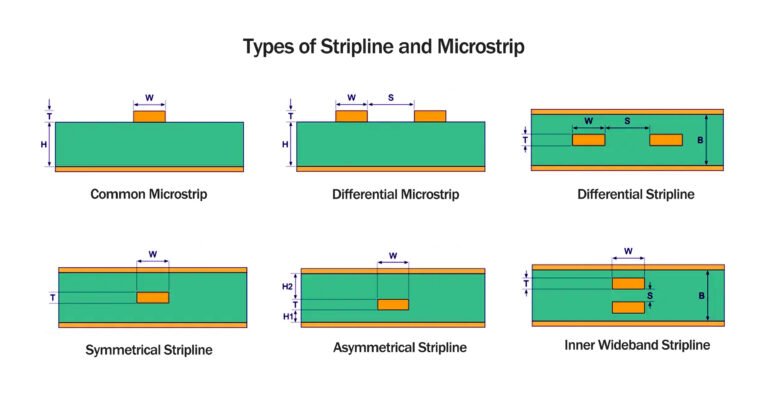
Types of Stripline and Microstrip
1. Microstrip Line Subtypes
Microstrips are categorized by their geometric configurations, dielectric environments, and application-specific requirements:
a. Basic Microstrip
- Structure: Single conductor trace on the PCB surface with a single ground plane below.
- Field Distribution: Quasi-TEM mode (electric fields partially in air and dielectric).
- Applications: Low-cost RF/microwave circuits (e.g., Wi-Fi antennas, RF filters).
b. Embedded Microstrip
- Structure: Trace embedded under an additional dielectric layer (e.g., solder mask), reducing radiation.
- Advantage: Lower EMI compared to basic microstrips while retaining surface accessibility.
- Applications: Consumer electronics (e.g., Bluetooth modules).
c. Differential Microstrip Pair
- Structure: Two closely spaced traces on the surface, with a shared ground plane.
- Field Distribution: Electric fields concentrated between the two traces (differential mode).
- Impedance: Typically 90–100 Ω, controlled by trace width (w), spacing (s), and dielectric thickness (h).
- Applications: High-speed digital signals (e.g., USB 3.0, HDMI).
d. Coplanar Microstrip
- Structure: Trace surrounded by parallel ground planes on the same layer.
- Advantage: Natural shielding against adjacent traces; used in high-density layouts.
- Applications: mmWave circuits (e.g., 5G front-ends).
e. Suspended Microstrip
- Structure: Dielectric substrate elevated above the ground plane, creating an air gap.
- Advantage: Reduced dielectric loss and increased characteristic impedance.
- Applications: High-power RF amplifiers (e.g., satellite transponders).
2. Stripline Subtypes
Striplines are classified based on symmetry, dielectric layers, and routing complexity:
a. Basic Stripline
- Structure: Trace sandwiched between two ground planes, fully enclosed by dielectric.
- Field Distribution: Pure TEM mode (fields confined to dielectric).
- Applications: High-speed digital backplanes (e.g., PCIe 5.0).
b. Symmetric Stripline
- Structure: Trace centered between two identical ground planes.
- Advantage: Balanced impedance and minimal crosstalk.
- Applications: Differential signal routing (e.g., Ethernet 10GBASE-KR).
c. Asymmetric Stripline
- Structure: Trace offset toward one ground plane, altering impedance and capacitance.
- Use Case: Matches impedance in hybrid layer stacks (e.g., combining FR4 and Rogers substrates).
d. Differential Stripline Pair
- Structure: Two traces embedded between ground planes, routed with tight spacing.
- Field Distribution: Fields contained within the dielectric, minimizing EMI.
- Impedance: Typically 100 Ω, calculated using trace width (w), spacing (s), and dielectric thickness (h).
- Applications: High-speed serial links (e.g., SATA 6 Gb/s).
e. Coplanar Stripline
- Structure: Trace with parallel ground planes on the same internal layer.
- Advantage: Simplified routing in multi-layer PCBs.
- Applications: High-frequency mixers (e.g., radar receivers).
f. Wideband Stripline
- Structure: Thick dielectric layer with a wide trace, optimized for low loss across broad bandwidths.
- Applications: Test equipment (e.g., oscilloscope probes).
3. Hybrid Variations
Some designs combine microstrip and stripline elements for specific needs:
a. Microstrip-to-Stripline Transition
- Purpose: Connect surface-mounted components (e.g., SMA connectors) to embedded traces.
- Design: Tapered transitions with via fences to minimize reflections.
- Applications: RF front-ends in mobile phones.
b. Embedded Stripline with Microstrip Overlay
- Structure: Stripline trace covered by a microstrip layer for additional shielding.
- Use Case: High-reliability systems (e.g., aerospace avionics).
4. Contrast with Other Transmission Lines
While the focus is on microstrip and stripline, other types are mentioned in the documents:
| Type | Structure | Key Feature |
|---|---|---|
| Coplanar Waveguide | Trace with side-by-side ground planes on the same layer | Easy impedance tuning for RF circuits; natural shielding |
| Slotline | Signal propagates through a slit in a ground plane | Used in microwave antennas and balanced circuits |
| Parallel-Plate Waveguide | Two parallel conductive plates with a dielectric in between | Broadband, low-loss performance; high-power applications |
Key Takeaways
- Microstrip Variants prioritize accessibility, radiation efficiency, and cost.
- Stripline Variants emphasize shielding, impedance precision, and high-frequency stability.
- Hybrid Designs leverage both structures for complex systems (e.g., automotive radar, medical imaging).
Electrical Characteristics: Impedance, Loss, and Speed
Characteristic Impedance
Microstrip Impedance:
Where:
-
-
Microstrips offer a wider impedance range (20–120 Ω) but require broader traces for the same impedance compared to striplines.
Stripline Impedance:
Where:
-
-
-
-
Striplines support higher impedances (35–250 Ω) with narrower traces, thanks to the fully dielectric environment.
When calculating the characteristic impedance of microstrip and stripline, leveraging professional tools enhances design accuracy. Visit PCB Impedance Calculator to input parameters like dielectric constant and trace width, and get real-time impedance values (supports microstrip, stripline, and differential pair calculations), avoiding errors from manual formula derivation.
Signal Loss and Velocity
Microstrip Signal Velocity:
Where:
-
-
-
Stripline Signal Velocity:
Losses are primarily from conductor resistivity and dielectric damping, with no radiation loss. The fully dielectric environment slows signal velocity but ensures consistent performance.
Where:
-
-
-
Design Considerations and Manufacturing
Layer Stackup and Cost
- Microstrips are cheaper and simpler to fabricate, requiring only two layers (signal and ground). They are ideal for surface-mount components and easy troubleshooting.
- Striplines demand multilayer PCBs, increasing manufacturing complexity and cost. They are routed on internal layers, necessitating vias for connectivity but offering superior shielding.
Impedance Control and Crosstalk
- Microstrips are prone to crosstalk and EMI due to their exposed structure. Designers use guard traces or ground pours for mitigation.
- Striplines inherently suppress crosstalk and EMI via dual ground planes, making them critical for high-speed signals (e.g., GHz-range data buses).
Applications and Practical Guidelines
When to Use Microstrip
- Low-to-medium frequency circuits (e.g., antennas, RF filters, and low-power transceivers).
- Cost-sensitive designs requiring surface accessibility.
- High-speed signals prioritizing velocity over shielding (e.g., differential pairs with controlled impedance).
When to Use Stripline
- High-frequency/high-speed systems (e.g., microwave amplifiers, radar modules, and backplanes).
- EMI-sensitive environments (e.g., medical devices, aerospace electronics).
- Precision impedance control for matched networks and low-loss transmission.
Applications and Practical Guidelines
Case Study 1: Microstrip in 5G Antenna Arrays
Scenario: A 5G base station antenna array requires compact, low-cost transmission lines for phase-shifting networks.
Solution: Microstrips are used for radiating elements and feedlines due to their exposed structure, which enables coupling with air for radiation. For example, Samsung’s 5G Massive MIMO Antenna employs microstrips with a Rogers RT/duroid 5880 substrate (εr=2.2) to achieve 28 GHz operation. The quasi-TEM mode allows engineers to adjust impedance (50 Ω) via trace width (w=0.3 mm, h=0.762 mm), balancing radiation efficiency and cost.
Advantage: Microstrips eliminate the need for expensive shielded layers, reducing weight and fabrication complexity in antenna arrays.
Case Study 2: Stripline in High-Speed Data Centers
Scenario: A 400G Ethernet switch motherboard demands low-latency, EMI-free signal routing for backplane connections.
Solution: Striplines are embedded in the motherboard’s inner layers to route differential pairs (e.g., PCIe 5.0, 32 GT/s). For instance, Intel’s Ice Lake Server Chipset uses striplines with an FR4 core (εr=4.4) and 100 Ω differential impedance. The dual ground planes suppress crosstalk between 100+ high-speed channels, ensuring BER < 10^-12 at 25 GHz.
Advantage: Striplines’ TEM mode minimizes dispersion, critical for maintaining signal integrity over 30 cm backplane traces.
Case Study 3: Hybrid Microstrip-Stripline in Automotive Radar
Scenario: A 400G Ethernet switch motherboard demands low-latency, EMI-free signal routing for backplane connections.
Solution: Striplines are embedded in the motherboard’s inner layers to route differential pairs (e.g., PCIe 5.0, 32 GT/s). For instance, Intel’s Ice Lake Server Chipset uses striplines with an FR4 core (εr=4.4) and 100 Ω differential impedance. The dual ground planes suppress crosstalk between 100+ high-speed channels, ensuring BER < 10^-12 at 25 GHz.
Advantage: Striplines’ TEM mode minimizes dispersion, critical for maintaining signal integrity over 30 cm backplane traces.
Case Study 4: Stripline in Medical MRI Equipment
Scenario: A 3T MRI scanner’s transceiver coil demands ultra-low loss and EMI isolation to detect faint biological signals.
Solution: Striplines with a PTFE dielectric (εr=2.1) are used for RF coil connections, enclosed in copper-clad layers to prevent interference with the magnetic field. GE Healthcare’s SIGNA™ MR System employs 50 Ω striplines with h=0.5 mm and w=0.1 mm, achieving Q-factors > 1000 at 128 MHz.
Advantage: Striplines’ shielding eliminates crosstalk between 32 receiver channels, critical for high-resolution imaging.
Case Study 5: Microstrip in Consumer Wi-Fi Routers
Scenario: A Wi-Fi 6 router (802.11ax, 2.4/5 GHz) requires cost-effective signal routing for multiple antennas.
Solution: Microstrips on a 4-layer FR4 PCB (εr=4.4) connect the SoC (e.g., Qualcomm IPQ8074) to surface-mounted diplexers and antennas. The traces (w=1.2 mm, h=1.6 mm) achieve 50 Ω impedance with <0.5 dB loss at 5 GHz.
Cost Savings: Microstrips reduce layer count by 50% compared to striplines, cutting PCB costs from $25 to $15 in high-volume production.
Conclusion
Stripline and microstrip represent two pillars of PCB transmission line design, each optimized for distinct scenarios. Microstrips excel in simplicity, cost-effectiveness, and moderate performance, while striplines deliver superior shielding, signal integrity, and high-frequency capability. By evaluating factors like frequency, impedance requirements, and environmental constraints, engineers can select the optimal structure to balance performance and practicality in modern electronics.
In summary, choosing between microstrip and stripline requires balancing impedance needs with cost considerations. We suggest using PCB Impedance Calculator for design assistance—input material and geometric parameters to get characteristic and differential impedance values in one click, boosting high-speed PCB design efficiency.
Final Tip: For hybrid designs, combine both structures: use microstrips for surface-mounted components and striplines for internal high-speed routing, leveraging their complementary strengths.