Identify the Device and Clock Configuration
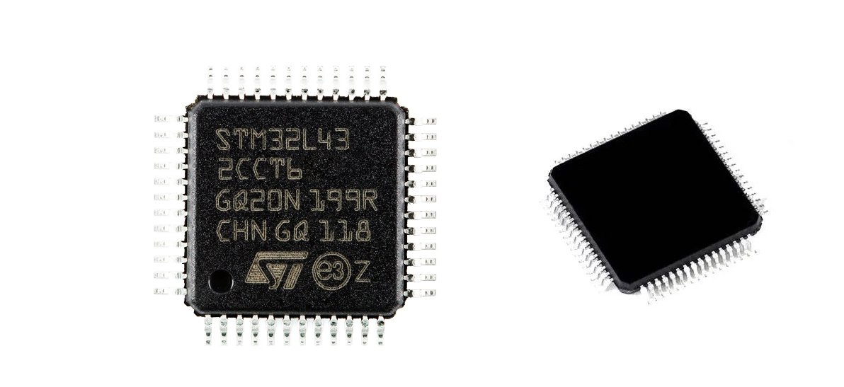
The STM8S207C8 is an 8-bit STM8 microcontroller. Before planning maintenance or a replacement, record the complete package marking, board revision, supply arrangement and clock components. A family name alone is not enough to select a pinout or memory layout.
ST’s STM8S207/208 datasheet lists the C8 device with 64 KB of program Flash, 6 KB of RAM and 1536 bytes of data EEPROM. The C8 package has 48 pins and 10 ADC channels. The maximum CPU frequency is 24 MHz; the internal high-speed RC oscillator is 16 MHz. These are different specifications. Determine the board’s actual clock source and divider configuration before calculating timer periods or communication rates.
Map Flash, EEPROM and Option Bytes
For the C8 device, program Flash occupies 0x008000–0x017FFF. RAM occupies 0x000000–0x0017FF, and the 1536-byte data EEPROM occupies 0x004000–0x0045FF. EEPROM, option bytes and program Flash have different purposes; a program binary does not necessarily include the board’s calibration values or configuration.
Record the start address and length of each available file, along with the tool’s address convention. A raw binary needs an explicit load address. Application boundaries should come from a linker map, documented update format or verified image analysis. Do not assume a separate security region or treat 0x800000 as this device’s Flash base.
Use the Documented SWIM Interface
STM8S207C8 uses the single-wire interface module, SWIM, for supported programming and debugging. The signal is multiplexed on PD1/SWIM. Confirm its physical pin using the exact package drawing, then trace the board connection. Check ground, reset, supply reference and the programming tool’s connection requirements before attaching a probe.
A connector that resembles another board’s debug port does not establish its pinout. JTAG scripts and STM32-specific protection registers are not substitutes for the STM8 documentation. ST’s peripheral list does not specify a dedicated hardware AES engine for this device; any encryption used by an application must be established from that application’s design or firmware evidence.
Build a Motion-Control Signal Map
For a motion-control board, start with a schematic or a measured net map. Identify timer outputs, driver enable and fault lines, feedback inputs, limit switches and command interfaces. Verify each signal against both the MCU pin assignment and the surrounding circuitry; an available peripheral function does not prove the board uses it.
Under controlled test conditions, record PWM frequency, duty range, polarity, startup order and the response to documented inputs. Capture the clock configuration and test conditions alongside waveforms so another engineer can interpret the timing. Distinguish measured behavior from a hypothesis about the control algorithm. Use an appropriate bench setup before evaluating outputs that could drive a motor or other actuator.
Protect Original Firmware During Assessment
Readout protection is an access-control feature, not evidence that the firmware is AES-encrypted. ST’s RM0016 reference manual, section 4.5.1, explains that removing readout protection automatically erases program Flash, data EEPROM and option bytes. A tool offering to remove protection can therefore conflict with a requirement to preserve the original contents.
Check the protection state and the documented effect of any proposed operation before proceeding. If preservation is required, stop at an erase or unprotect prompt and look for owner-supplied source code, production binaries, update packages or verified backups. Assess supported access only with authorization; do not promise recovery from a protected device.
Create a Reproducible Assessment Record
Keep a record of the device marking, board revision, wiring, supply and clock conditions, tool and software versions, access state, file address ranges and checksums. Include original captures and explain how each conclusion was reached. A file hash can show that two copies match; it does not by itself establish firmware authenticity, completeness or correct operation.
This article provides a documentation-based assessment framework. It does not report a completed recovery, a tested protection bypass or results from a fleet of controllers. Those claims would require project-specific records, including test conditions and independently checkable results.
Validate a Maintenance or Replacement Plan
Where approved firmware and a suitable test board are available, compare startup behavior, communications, enable and fault handling, timing limits and documented operating requirements before deployment. Preserve calibration and configuration data through the approved maintenance process.
Access to a firmware file alone does not reconstruct the complete system. Driver circuitry, sensor scaling, mechanical limits and closed-loop tuning can all affect a replacement design. State what has been verified, what remains inferred and which tests are still needed before accepting a maintenance plan.
Discuss an STM8 board assessment:

Principal Engineer:
Dr. Billy Zheng
Well Done PCB Technology
billy@reversepcb.com
Emergency Support: +86-157-9847-6858