PIC18F14K50 Datasheet Checks Before Board Release
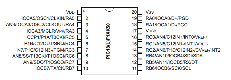
Use the datasheet for the complete PIC18F14K50 ordering code and package, then cross-check it against both the schematic symbol and firmware configuration. The family name alone is not enough to confirm pin placement, USB clocking, programming access, or electrical limits. Before committing the PCB, compare the silicon revision and current errata with the features in use. A useful bring-up image should first prove ICSP identification, reset, and a stable system clock before enabling USB or high-current outputs.
- Power network: connect every specified supply and ground pin, place local decoupling at the package, and implement the required
VUSBcapacitor exactly as shown for the internal USB regulator. - USB clock domain: verify the oscillator source, PLL settings, and configuration bits that produce the clock required by the USB module over voltage and temperature.
- Programming access: keep
MCLR/VPP, ICSP clock, ICSP data, supply, and ground accessible without loads that violate programming levels. - Pin multiplexing: reconcile USB, analog, timer, and serial functions with the package pin table before assigning GPIO in firmware.
- Electrical margins: check absolute maximum ratings separately from recommended operating limits, including pin current, port current, and ADC source impedance.
PIC18F14K50 Overview
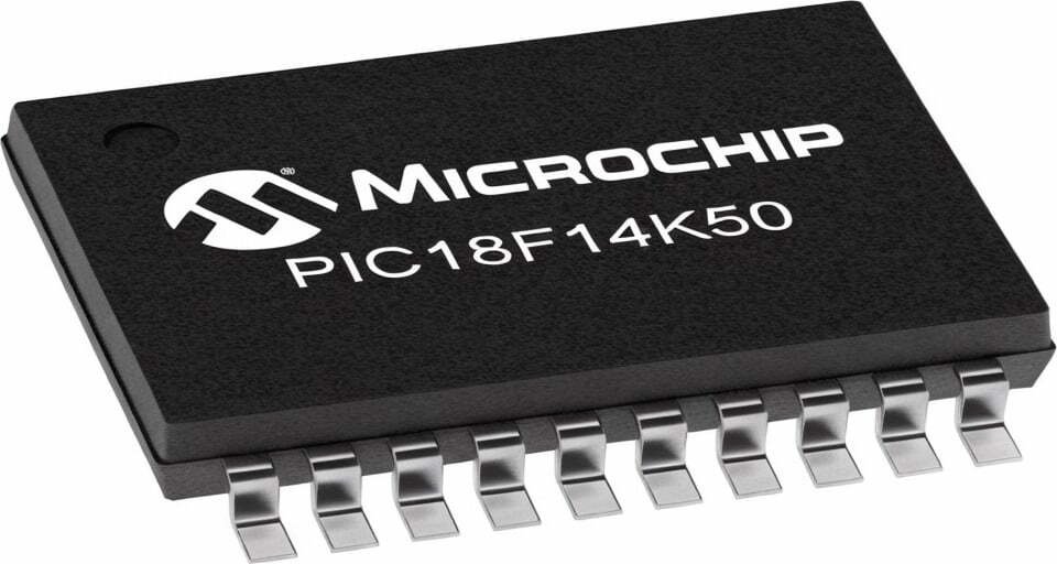
PIC18F14K50 is a low-cost microcontroller with advanced features and special value in the embedded USB market. It has a full-speed USB 2.0 compatible interface that can automatically change clock sources and power levels, making it ideal for battery-powered applications.
PIC18F14K50 Features
Processing power:
- High-performance PIC18 core
- Architecture optimized for C compiler
- 8×8 single-cycle hardware multiplier
- Dual capture/compare/PWM interface – up to 5 PWM outputs – programmable dead time, auto-shutdown/restart
- Memory and data storage:
- 256-byte dual-access RAM with flexible clock options
- Communication interfaces:
- USB V2.0 compatible interface
- Master I2C/SPI interface – supports all 3-wire SPI modes – address mask I2CTM compatible Master and Slave modes
- Enhanced addressable USART module – supports RS-485, RS-232, and LIN2.0
- Analog and digital input/output:
- 10-bit, 9-channel ADC module – can sample and convert automatically – can operate in sleep mode
- mTouchTM touch-compatible analog comparator W/SR latch – Rail to Rail operation – independent input multiplexing
- Programmable on-chip voltage reference – versatility for operation with comparators or ADCs
- Power management:
- Software-programmable under-voltage reset function
- Four power management operating modes
- Dual-speed clock start-up option
- Other features:
- Self-programming under software control
- Support for interrupt priorities
- Programmable period enhanced watchdog timer for full-speed UART
- Supports low-speed and full-speed operation
- Supports control, interrupt, synchronous, and bulk transfers
- Up to 16 endpoints (or 8 bidirectional)
- Automatic detection of physical connection to USB host
- Can operate at up to 48MHz internal frequency
- Fully adjustable internal oscillator – adjustable frequency drift
- Internal 4X Phase-Locked Loop (PLL) – can use external or internal oscillator
- Fail-safe clock monitor – can safely shut down during oscillator failure
PIC18F14K50 Parameters
- CPU Speed: 48 MHz
- 16K bytes of flash memory
768 bytes of RAM - 256 bytes of data EEPROM
- Size: 16 KB
- RAM Size: 768 B
- Number of I/O Pins: 18
- Operating Voltage Range: 1.8 V to 5.5 V
- 25 mA GPIO sink/source current
- Package/Case: PDIP20, SOIC20, SSOP20, QFN20
PIC18F14K50 Pinout
the PIC18F14K50 is available in four different packages with different pinouts: PDIP20, SOIC20, SSOP20, and QFN20.