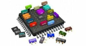
System-on-Chip (SoC) Technology
SoC basics: architecture, components (CPU/GPU/NPU), and applications in mobile/IoT. Learn to design with Arm/AMD SoCs. Industry insights inside!
Schematic & Gerber restoration
MCU/CPLD code restore access & backup
1:1 exact hardware replication
BLE & Classic BT wireless solutions
Precision PID & thermal management
High-efficiency motor drive control
Industrial RS485/RTU communication
Custom STM32/ESP32 firmware & HW
Calculate the PCB trace width based on temperature rise, current, and copper thickness (IPC-2152).
IC reverse engineering is a sophisticated process of hardware design analysis and firmware recovery. It involves the detailed study of integrated circuits or microcontrollers to understand their architecture, logic, and embedded firmware. This professional service is essential for legacy system maintenance, hardware forensics, and interoperability research, allowing engineers to recover critical data from older or unsupported components.
Delayering circuits through chemical etching or mechanical polishing.
Using high-res SEM imagery to extract transistor-level connectivity.
“It is not just duplication; it is a vital tool for deep understanding of advanced nodes and patent protection.”
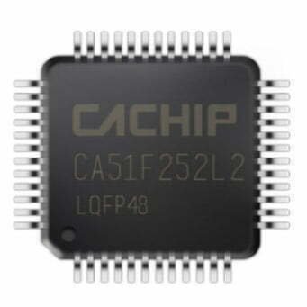


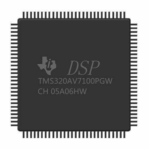
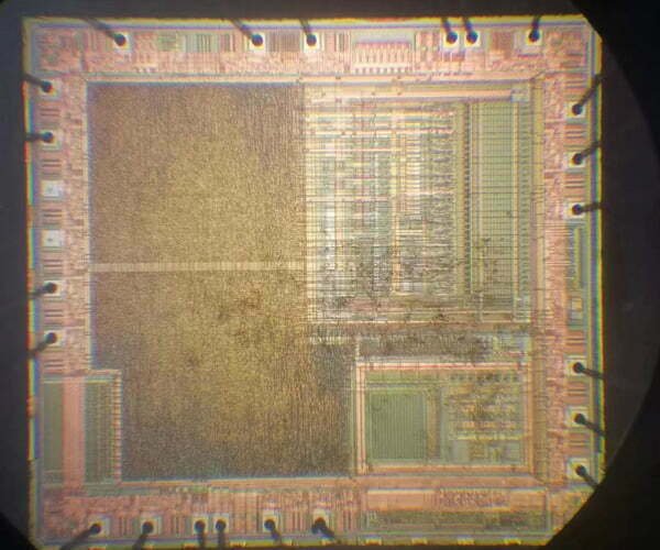
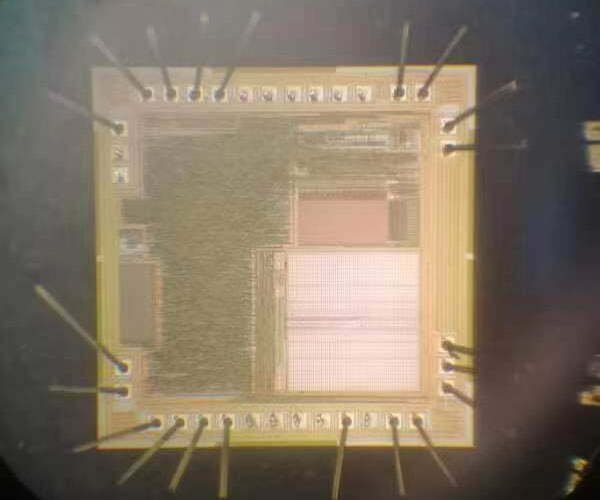
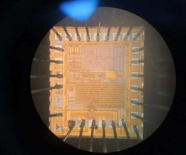
With over 15 years of experience, we have completed 1,000+ hardware analysis and firmware recovery projects. Our clients range from innovative startups to global enterprises in industries such as Automotive, Aerospace, Industrial Automation, Medical Devices, and Telecommunications. We are the preferred partner for businesses requiring deep-level hardware insights and legacy system support. For more IC models, please contact us directly.
Our professional methodologies for chip analysis and data recovery.

We utilize advanced protocol analysis to identify logical sequences within firmware. By analyzing execution timing and erase sequences in legacy architectures like the ATMEL AT89C series, we identify states where memory becomes accessible. Our team maps firmware structures by detecting data patterns, such as FFFF hex sequences, ensuring successful recovery or migration to modern hardware platforms.
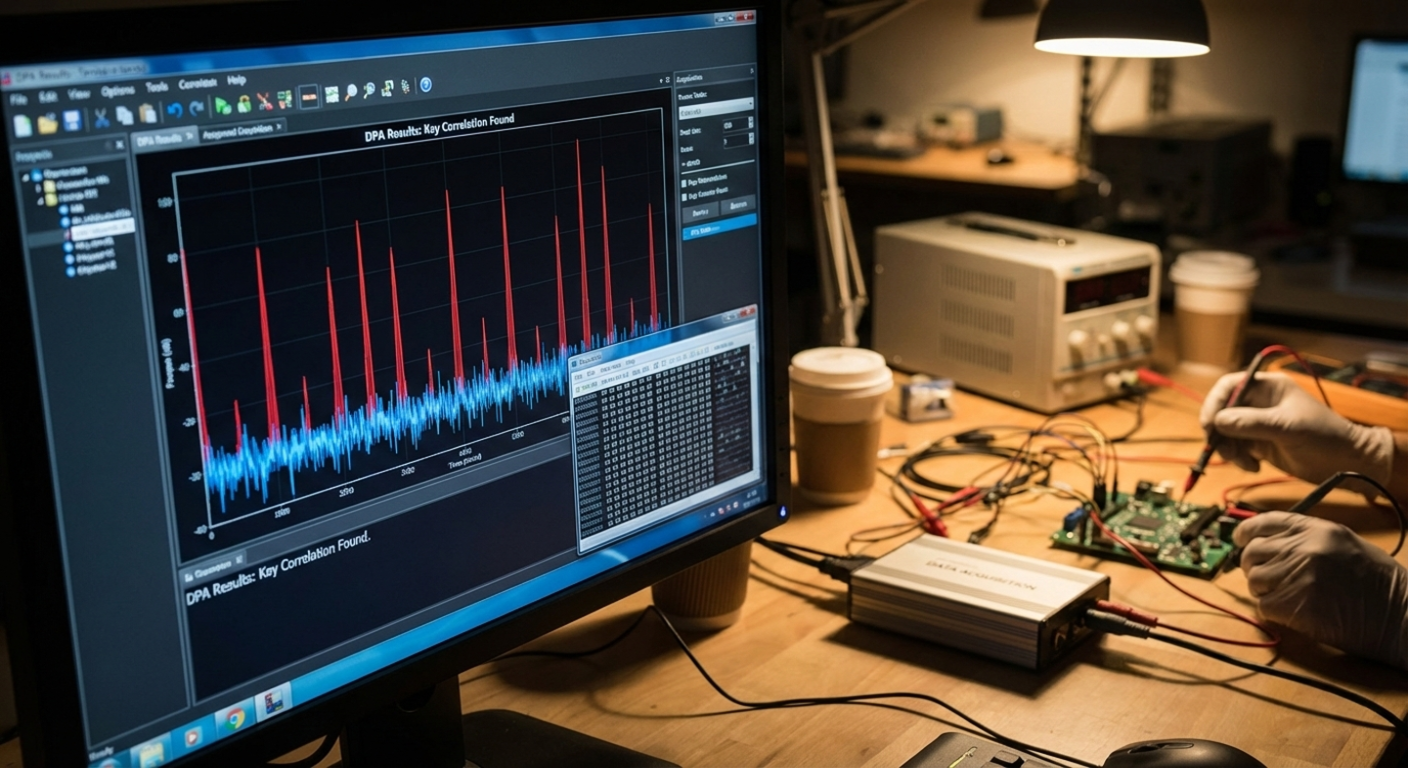
This non-invasive technique monitors power consumption and electromagnetic emissions during chip operation. By applying advanced statistical models, we can infer logic states and execution patterns without physical intrusion. This methodology is crucial for understanding internal device operations and cryptographic processes, providing a deep look into the chip’s functional behavior and data flow.
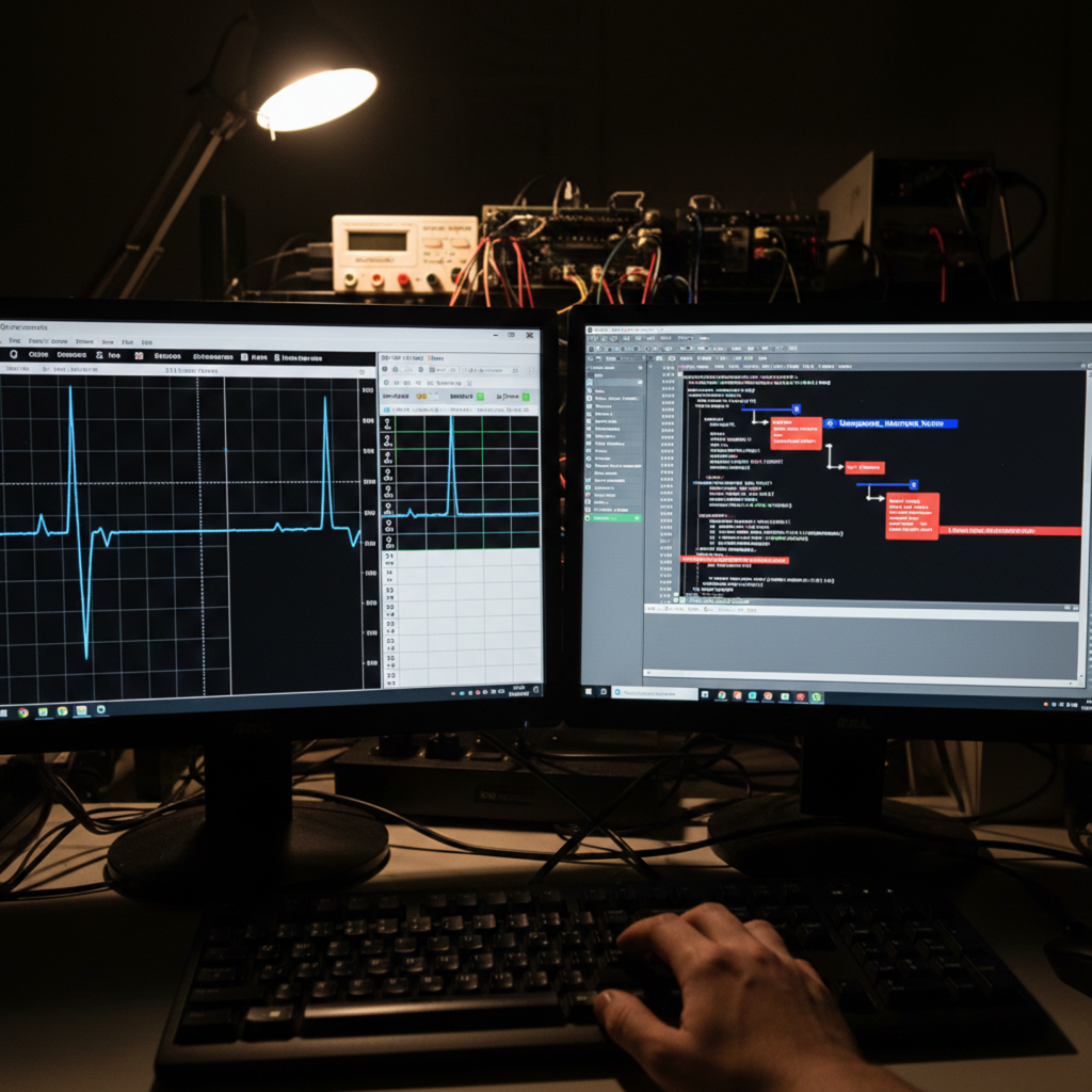
By applying controlled voltage glitches or clock transients, we analyze processor behavior under abnormal operational conditions. This stress methodology helps in identifying hidden design vulnerabilities and improving overall system robustness. It allows engineers to pinpoint critical failure points and reconstruct control flow logic that only emerges during specific environmental fluctuations or hardware exceptions.
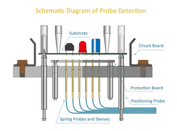
Using high-precision sub-micron probe stations, we perform signal extraction directly from the IC’s internal metal wiring. This physical approach allows for real-time functional verification and precise data path mapping. By bypassing external security pins and interfacing directly with the internal bus, we can observe instruction execution and register states that are otherwise invisible to external debugging tools.

Specialized UV irradiation methods are employed for analyzing One Time Programmable (OTP) memory structures. This technique enables the recovery of data for legacy system migration by manipulating the floating gate charges. It is an essential service for restoring firmware from discontinued industrial chips where original code is lost, providing a reliable pathway for maintaining critical infrastructure and legacy hardware.

We leverage architectural design characteristics for advanced data recovery. By identifying specific hardware flags or logical flip-flops (FFs) within the memory structure, we evaluate the chip’s state for precise firmware extraction. This methodology is highly effective for the ATMEL 51 (AT89C51) series, where byte-level analysis allows engineers to restore access to critical code lost to hardware obsolescence.
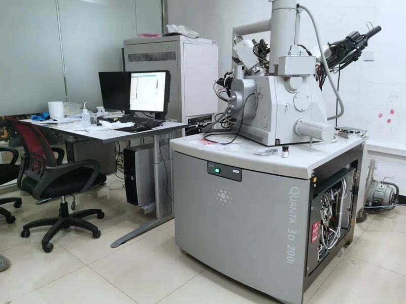
Focused Ion Beam (FIB) technology is our premier method for precision circuit restoration. After chemical decapsulation, we use electron microscopy to modify internal logic paths at the nanometer scale. This is ideal for TI MSP430 series (MSP430F1101A, F149, F425) projects involving security fuses. By restoring circuit states, we enable firmware recovery from protected devices when original source code is unavailable.
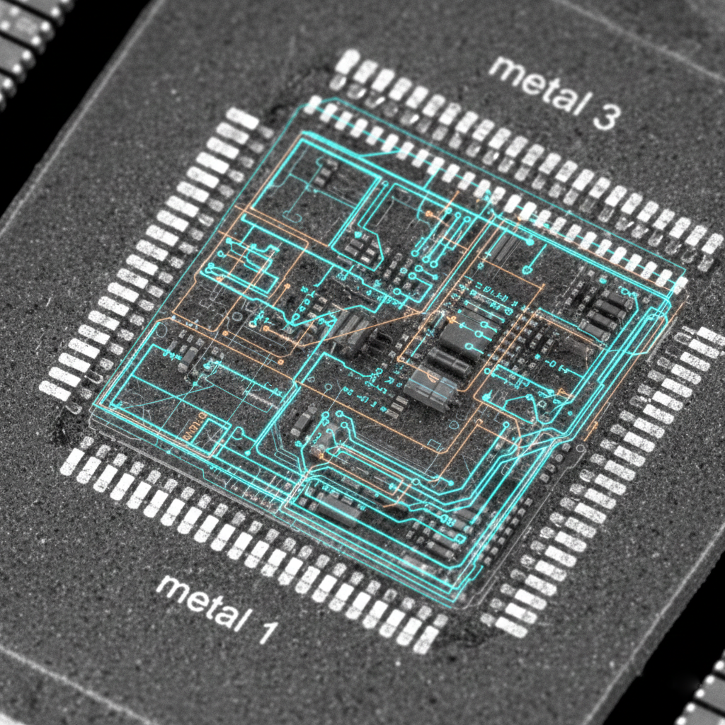
For high-complexity CPLD and DSP chips, we perform deep-level structural analysis to bypass non-functional logic gates and restore access to core system data. This process involves reconstructing complex netlists and identifying hidden signal paths within the silicon fabric. It is particularly effective for the TMS320 series, enabling researchers to recover proprietary processing algorithms for R&D purposes.
Simple decapsulation takes 1-3 days. Full netlist extraction can take 2-12 weeks depending on the chip’s complexity and node size.
Costs vary widely. A basic structural analysis might start at $5k, while full circuit extraction for advanced nodes can range from $50k to over $200k.
Yes, we have specialized techniques for reading non-volatile memory (Flash/EEPROM), though success depends on the specific security fuses and encryption used.

SoC basics: architecture, components (CPU/GPU/NPU), and applications in mobile/IoT. Learn to design with Arm/AMD SoCs. Industry insights inside!

What is IC Unlock? IC unlock is aslo called IC decrypt, IC attack or IC crack. An IC (integrated circuit) is usually encrypted when it
Are you looking for a comprehensive guide to programming STM32 microcontrollers? If so, you’ve come to the right place! STM32 microcontrollers are popular for their