What SMT Means in PCB Assembly — Beyond the Acronym
post views:2
Table of Contents
Ask an engineer “what is SMT” and you’ll usually hear “Surface Mount Technology.” That’s correct. But if you stop at the acronym, you miss what SMT actually means for how a PCB gets designed, built, tested, and paid for. This article explains the definition of SMT in terms that matter to anyone who designs, orders, or troubleshoots assembled circuit boards.
The Straightforward Definition of SMT
SMT (surface mount technology) is a PCB assembly method where components are mounted directly onto the surface of a printed circuit board, without leads passing through holes. This replaced through-hole technology (THT) as the dominant production method starting in the 1980s and now accounts for the vast majority of commercial PCB assembly.
The key distinction: in through-hole assembly, component leads go through drilled holes and get soldered on the opposite side. In SMT, components sit on top of pads printed with solder paste and are soldered in place during reflow. No holes, no lead trimming, and dramatically higher component density.
What “SMT” Changes About PCB Design
If you grew up on through-hole prototyping, moving to SMT means rethinking several design habits:
Trace routing gets tighter. SMD pads are smaller and closer together. You can place a decoupling capacitor within a millimeter of an IC power pin, which improves signal integrity in ways through-hole layouts rarely achieve.
Both sides become usable. SMT components can populate both the top and bottom of a board. This doubles the effective area without increasing the PCB outline, which matters a lot in compact consumer products.
Vias become routing tools, not component anchors. Since components don’t need plated through-holes, vias are freed up purely for layer transitions and thermal management.
Thermal design shifts. SMD components dissipate heat into copper planes through their pads rather than through lead wires. A proper copper pour under a power SMD part does more for cooling than a through-hole heatsink clip.
If you have already published an SMT-focused design and want to move it into production without redesigning the entire BOM, ReversePCB’s assembly service handles mixed-technology boards where SMT and through-hole components coexist.
SMT vs. Through-Hole: The Assembly Floor Reality
The definition of SMT matters most on the assembly line. Here is what changes when a design switches from through-hole to SMT:
Aspect
Through-Hole
SMT
Component placement
Manual or wave-solder fixtures
Automated pick-and-place at thousands of CPH
Soldering
Wave or hand soldering
Reflow oven with controlled thermal profile
Board real estate
Consumes both sides with lead holes
Components sit on surface, both sides usable
Minimum component size
~0805 equivalent
Down to 01005 (0.4 x 0.2 mm)
Rework difficulty
Easy with a soldering iron
Requires hot air, preheating, or dedicated rework station
Mechanical strength
Stronger (lead through hole)
Weaker against shear, relies on pad adhesion
For most production runs above a few dozen units, SMT wins on speed, consistency, and per-unit cost. The tradeoff is upfront tooling: stencil, pick-and-place programming, and reflow profiling all happen before the first board ships.
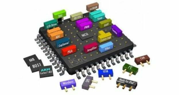
SMD Components: What Gets MountedSurface mount devices (SMDs) in close-up: chips, passives, and IC packages populate a dense PCB — each component type represents a decision about package size, thermal performance, and assembly complexity.
The components used in surface mount technology are called SMDs — surface mount devices. Common SMD package types include:
Passive chips (resistors, capacitors, inductors): Standards like 0402, 0603, 0805. The number is the footprint in hundredths of an inch — an 0603 measures 0.06″ x 0.03″.
SOIC, SSOP, TSSOP: Gull-wing-leaded ICs, the workhorses of analog and mixed-signal circuits.
QFP, LQFP, TQFP: Square ICs with leads on four sides, common on microcontrollers up to ~200 pins.
QFN, DFN: Leadless packages with exposed thermal pads underneath. Harder to hand-solder, excellent thermal performance.
BGA: Ball grid arrays hide solder balls under the package. Impossible to visually inspect after reflow without X-ray.
0201, 01005: Ultra-miniature passives used in phones and wearables. Hand-soldering is not realistic.
Choosing the right package is a manufacturing decision as much as an electrical one. If your contract manufacturer can’t reliably place 0201 parts, don’t specify them.
The SMT Assembly Process in Four Steps
Understanding the surface mount technology workflow helps you write better DFM rules:
Solder paste printing. A stainless-steel stencil aligns over the bare PCB. Solder paste is squeegeed across it, depositing paste only on component pads. Stencil thickness, aperture design, and paste rheology control the deposit volume.
Pick-and-place. A high-speed machine picks SMDs from tape reels or trays using vacuum nozzles and places them onto the pasted pads. Placement accuracy is typically better than 50 µm for modern machines.
Reflow soldering. The populated board travels through a reflow oven with controlled heating zones. The thermal profile ramps up, soaks to activate flux, spikes above liquidus (~217°C for SAC305 lead-free solder), then cools at a controlled rate. The paste melts, wets the pads and component terminations, and solidifies into reliable solder joints.
Inspection. Automated optical inspection (AOI) checks for solder bridges, tombstones, insufficient wetting, and component offsets. Boards with BGAs or hidden joints may also go through X-ray inspection.
If you are designing your first SMT board and want a manufacturing partner that catches DFM issues before prototyping, ReversePCB’s DFM review flags stencil, pad, and placement problems early.
Common SMT Defects and What They Tell You
Every SMT defect has a root cause. Learning to read them makes you faster at troubleshooting production issues:
Tombstoning: One end of a chip component lifts off the pad during reflow. Usually caused by uneven heating (one pad reaches liquidus first) or pad geometry imbalance. Fix: equalize pad sizes and thermal relief on both sides.
Solder bridging: Excess solder connects adjacent pads. Common causes: too much paste, stencil aperture too wide, or insufficient spacing between pads.
Insufficient wetting: The solder didn’t form a proper fillet. Check pad oxidation, paste age, or reflow profile — if the board never reached liquidus long enough, wetting fails.
Head-in-pillow: BGA balls and paste melt separately without merging. Usually a reflow profile issue where the package warps and the balls lose contact with paste during the liquid phase.
Voiding: Gas bubbles trapped in the solder joint beneath BGAs or QFNs. Excess flux, moisture, or an aggressive ramp rate can all cause voids.
Design Rules That Prevent SMT Headaches
If you follow these rules, your SMT yield will be measurably higher:
Pad-to-pad spacing: Keep at least 0.2 mm between adjacent pads unless your fab and assembler both approve tighter spacing.
Component-to-edge clearance: Parts within 3 mm of the board edge risk tombstoning from uneven heating near the rail. Move them inward or add thermal relief.
Fiducial marks: Place three global fiducials (one in each corner, asymmetrically) plus local fiducials near fine-pitch parts. Pick-and-place machines use these for optical alignment.
Stencil aperture reduction: For fine-pitch QFPs and 0.5 mm-pitch parts, reduce aperture width by 10–20% to prevent bridging. Your assembler’s stencil engineer should confirm this.
Thermal relief on large copper areas: A pad directly connected to a large ground plane will wick heat away during reflow, causing cold joints. Use thermal relief spokes.
SMT dominates PCB assembly, but it is not universal. Through-hole still wins in these scenarios:
Connectors and mechanical stress points. USB ports, barrel jacks, and terminal blocks experience repeated insertion force. Through-hole mounting provides mechanical anchoring that SMT pads cannot match.
High-power components. Large transformers, heat-sinked power transistors, and relay coils often use through-hole for both current capacity and thermal management.
Prototyping and one-off builds. Hand-soldering 0603 passives under a microscope is doable. Hand-soldering a 64-pin QFN is not. Through-hole prototyping remains faster for low-volume work.
Mixed-technology legacy designs. Many industrial and automotive boards combine SMT logic sections with through-hole power and I/O sections. These are fully manufacturable with today’s mixed-technology lines.
Frequently Asked Questions
What does SMT stand for?
SMT stands for Surface Mount Technology. It is the PCB assembly method where components mount directly onto the board surface rather than through drilled holes.
What is the difference between SMT and SMD?
SMT refers to the assembly technology (the process). SMD refers to the device (the component itself). An SMD, or surface mount device, is any component designed for SMT assembly.
Why did SMT replace through-hole for most PCB assembly?
SMT enables higher component density, automated high-speed assembly, smaller board sizes, and lower per-unit cost. It also allows components on both board sides, which through-hole cannot match.
Can you mix SMT and through-hole on the same board?
Yes. Mixed-technology boards are common in industrial and automotive electronics. The SMT side is reflowed first, then through-hole components are placed and wave-soldered or hand-soldered.
What is the smallest SMD component size?
01005 (0.4 x 0.2 mm) is the smallest widely-available passive size. These require specialized pick-and-place equipment and are primarily used in smartphones, wearables, and implantable medical devices.
What is the definition of SMT in electronics manufacturing?
In electronics manufacturing, the definition of SMT is an assembly process where solder paste is printed onto PCB pads, components are placed onto the paste by automated equipment, and the entire assembly passes through a reflow oven to form permanent solder joints without through-hole leads.