What is an RLC circuit?
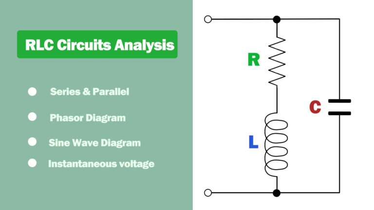
An RLC circuit is an electrical circuit that contains a resistor (R), inductor (L), and capacitor (C) connected in series or parallel. These components work together to store and transfer energy, leading to oscillations at a specific resonant frequency. RLC circuits are commonly used in various applications, including filters, oscillators, and tuning circuits.
Types of RLC Circuits
RLC circuits can be mainly divided into the following types:
RLC Series Circuit:
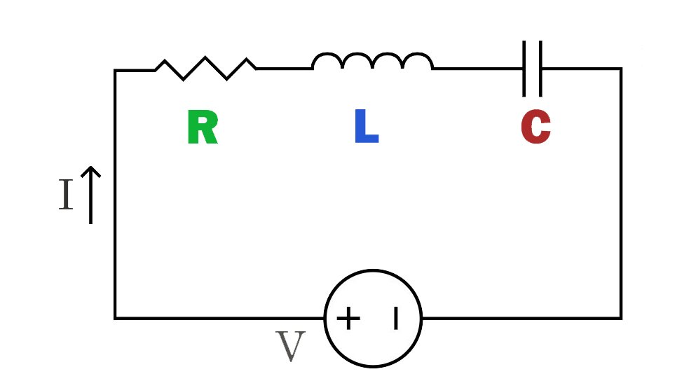
In this circuit, the resistor (R), inductor (L) and capacitor (C) components are connected in sequence on the same path. The current passes through the resistor, inductor and capacitor in sequence, causing the current to change accordingly in each component.
The series RLC circuit has the characteristics of frequency selectivity, presenting different impedance and response characteristics at different frequencies, so it is widely used in filters and tuned circuits.
RLC Parallel Circuit:
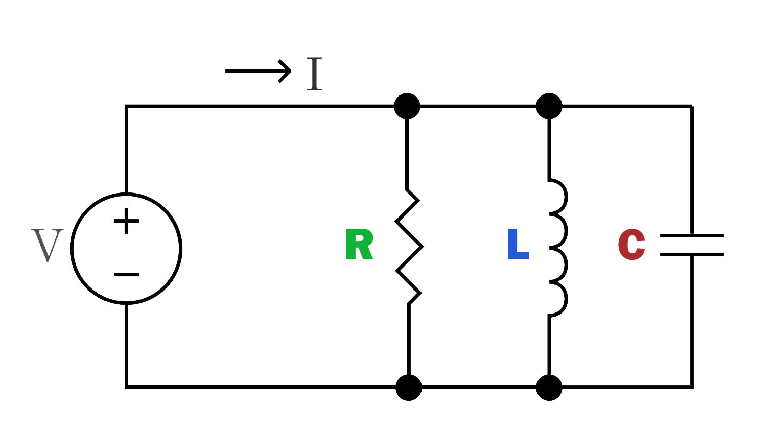
The parallel RLC circuit is to connect the resistor, inductor and capacitor in parallel paths respectively. The current is divided in the branches, and the voltage passing through each component is the same.
It circuit has impedance characteristics for current at a specific frequency, which can be used to selectively pass or block signals of certain frequencies.
How to Measure Voltage in the RLC Circuit?
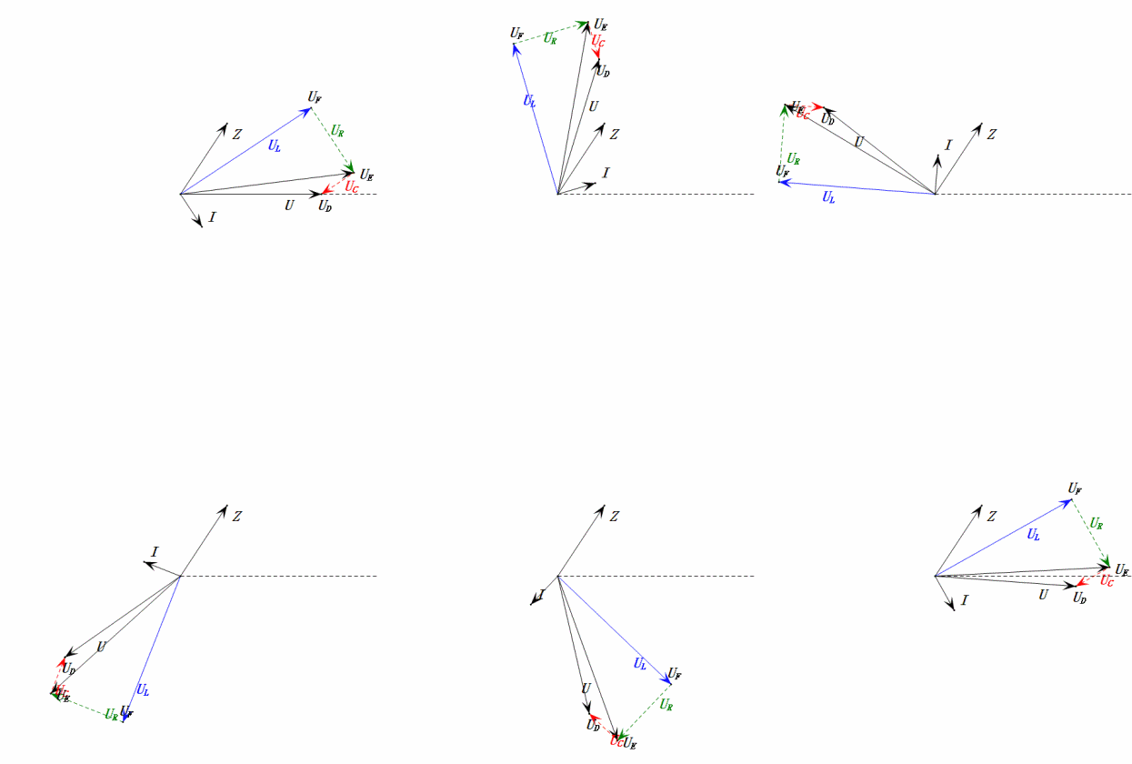
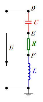
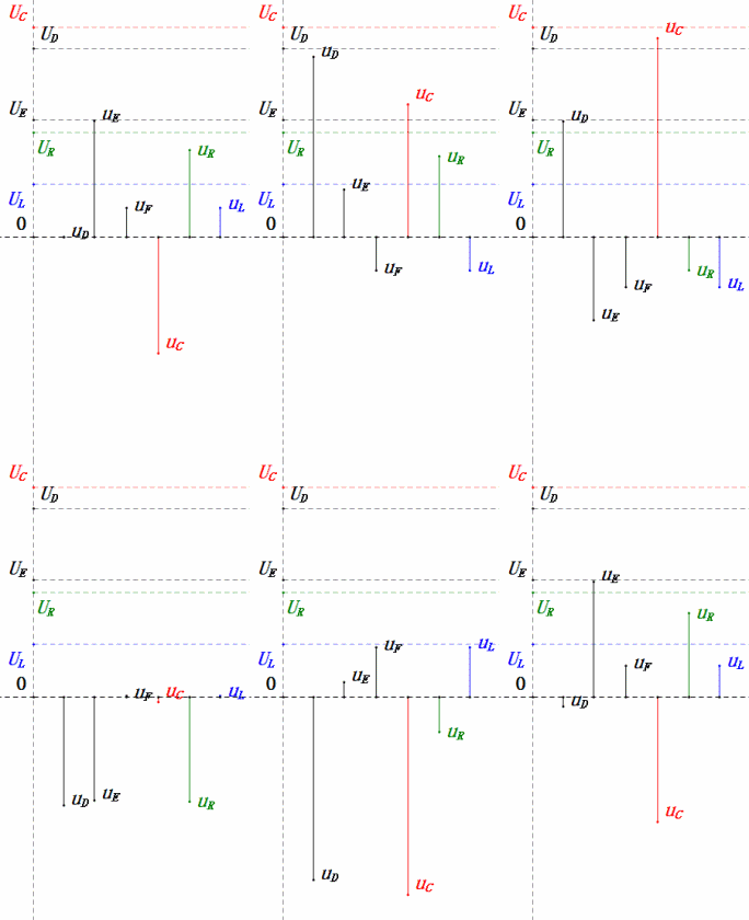
As below diagrams show:
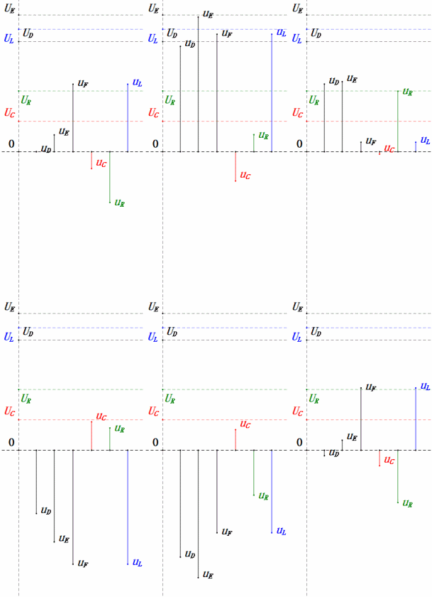
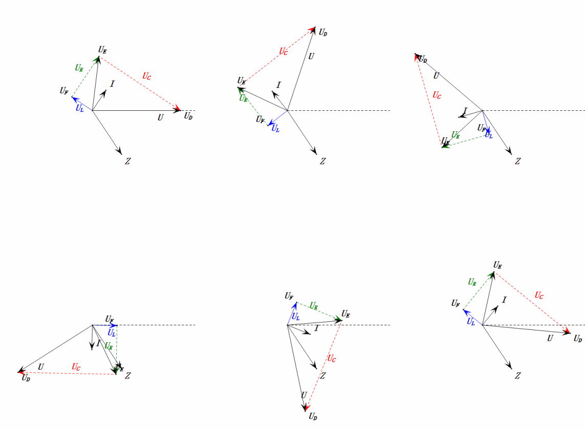
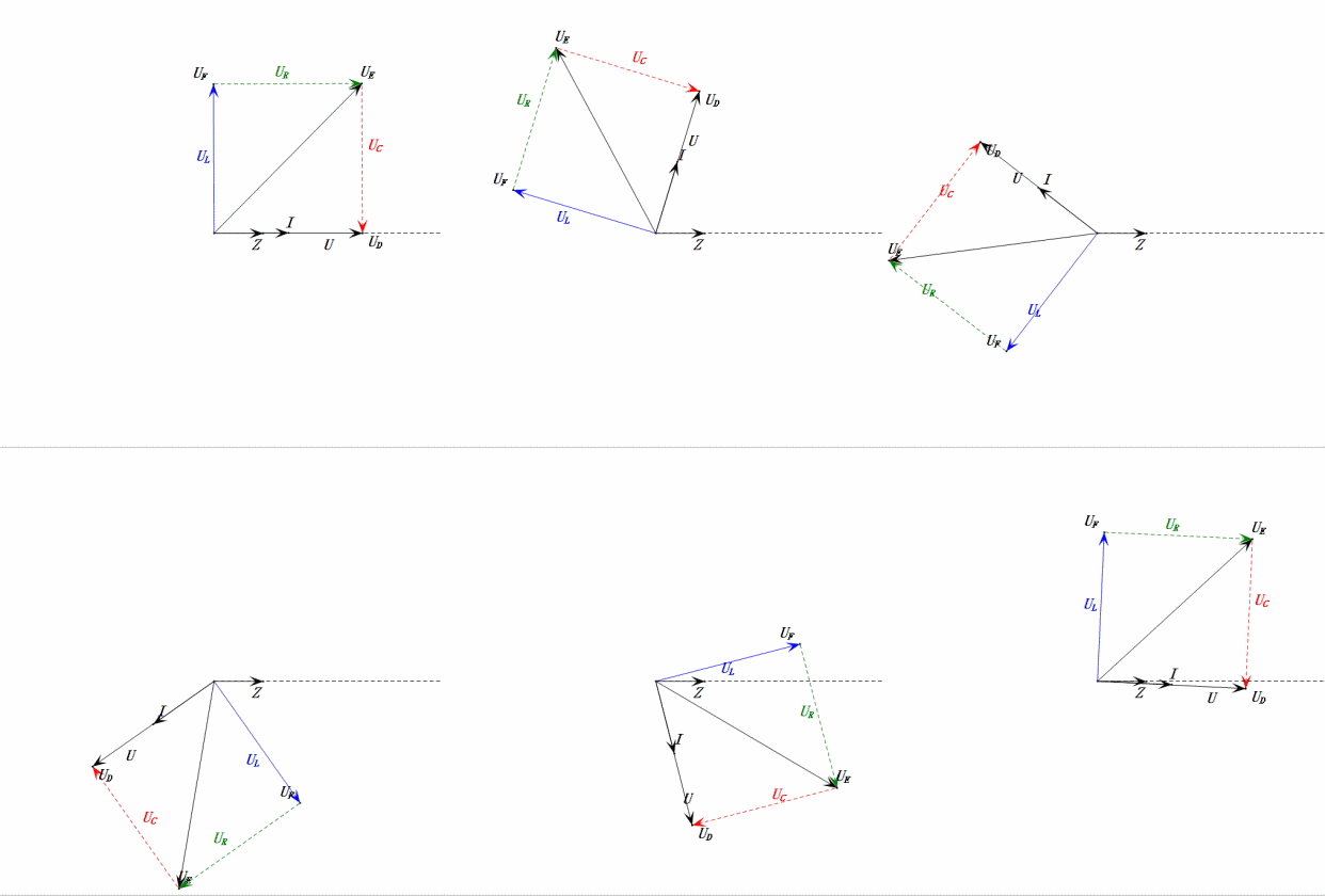
When U is a sinusoidal voltage, this circuit has three potential points D, E, and F. These three waveforms can be observed using an oscilloscope or measured with an AC voltmeter for UD, UE, UL, UR, and UC. The dynamic graph on the right reflects the changes in these five voltages over time in a certain scenario. In the dynamic graph, UF is equivalent to UL, and ideally, there should be another voltage UDF, but I have chosen not to include voltages with two-letter subscripts for simplicity.

Calculation Formula for Voltage
The phasor method is a brilliant solution that facilitates problem-solving but may cause us to miss out on the fascinating dynamic processes depicted in the graph above. With inductive reactance XL, resistance R, and capacitive reactance XC, the phasor method for solving this circuit is outlined as follows:
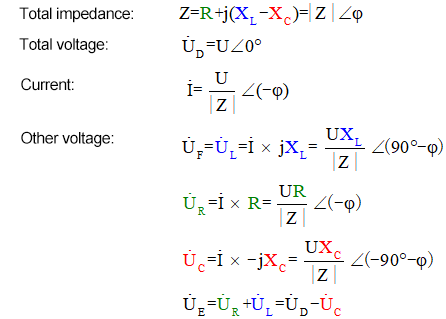
The AC voltmeter measures UR ≠ UE – UL. If L is an ideal inductor, these three will form a right triangle. Similarly, UC, UD, and UE will also form a triangle, though not necessarily a right one. This does not imply that Kirchhoff’s Voltage Law (KVL) is violated. If the instantaneous value u at a certain moment is measured, it will be found that uR = uE – uL and uC = uD – uE. Additionally, although current is not measured, the changes in UR are in phase with the changes in current.
Sine Signal Action and Resonance State
When a sine signal is applied, the inductive reactance XL = ωL and the capacitive reactance XC = (ωC)^-1. The state where these two are equal is known as resonance, allowing us to calculate a resonant angular frequency ω0.
In the next section, we will set the parameters to create phasor diagrams, static sine wave diagrams, and animations of the instantaneous value changes of voltage at 0.5ω0, ω0, and 2ω0.
Voltage under Different Resonant Angular Frequencies
Model Parameters:
- U = 6.00mV
- R = 2.00Ω (effective current less than 3.00mA, generally safe for components)
- C = 125μF
- L = 0.500mH
Calculated ω0 = 4000rad/s (corresponding to a frequency of approximately 637Hz, ignoring electromagnetic radiation effects for modeling convenience. Phasor diagrams and sine wave diagrams use RMS values; for peak values, multiply by 1.414)
Dynamic Voltage under 0.5ω0
After calculations, we can draw the phasor diagram and static sine wave diagram at the initial moment:
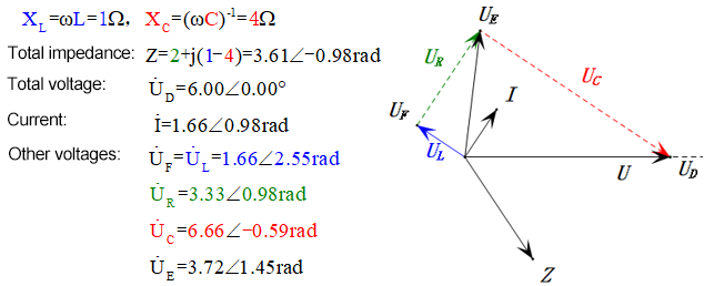
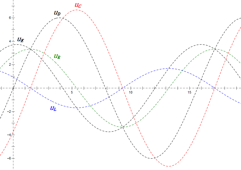
Analysis:
- Maximum current ≈ 1.57mA, safe for components.
- Phasor diagram forms a right trapezoid with UDF not considered.
- At 0.5ω0, XL < XC → smaller UL, larger UC. Maximum uC exceeds power supply voltage, potentially damaging the capacitor.
- uC lags uD by ≈30°; charging begins during uD’s rising phase, ending when uR = 0.
- Sine wave diagram shows uR = uE – uL and uC = uD – uE at every moment.
Dynamic Voltage under 1ω0
After calculations, we can draw the phasor diagram and static sine wave diagram at the initial moment:
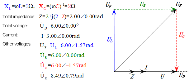
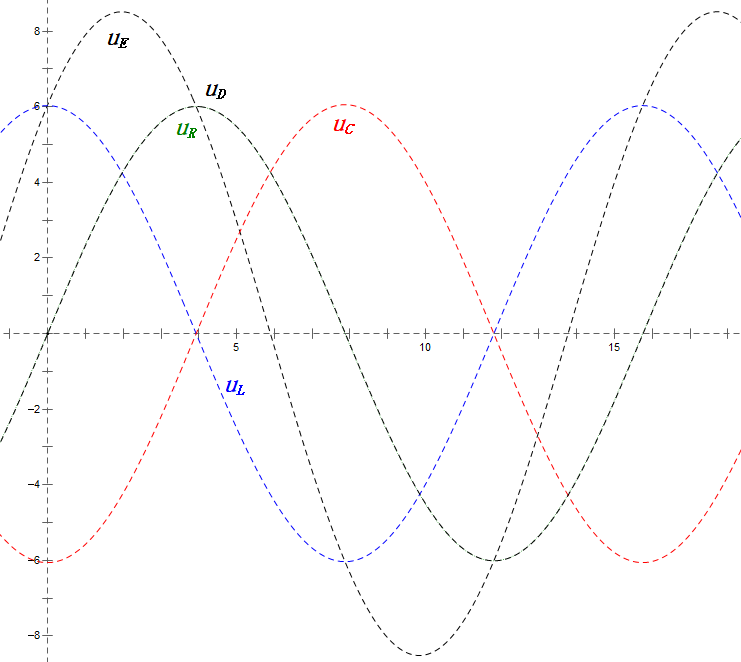
Analysis:
- Maximum current ≈ 4.24mA, safe for components.
- Phasor diagram forms a square at resonance (XL = XC).
- Maximum uE exceeds power supply voltage, but component impact unclear.
- Coincidence: XL = XC = R → uL and uC cancel each other in sine wave diagram, but current changes affect amplitudes.
- Impedance minimized, current maximized at resonance due to “maximum current” effect.
- uC lags uD by exactly 90°; charging begins when uD peaks and ends when uR = uD = 0.
- Sine wave diagram segments represent half the time of Case 1.
- Maximum UD = UR, UL = UC due to parameters, but all four voltages equal is a coincidence.
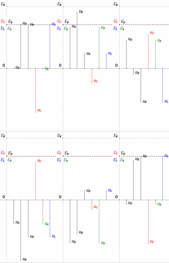
Dynamic Voltage under 2ω0
After calculations, we can draw the phasor diagram and static sine wave diagram at the initial moment:
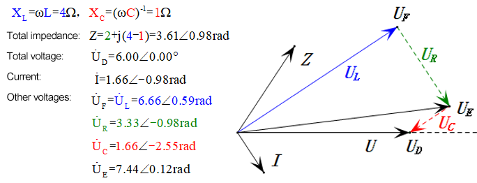
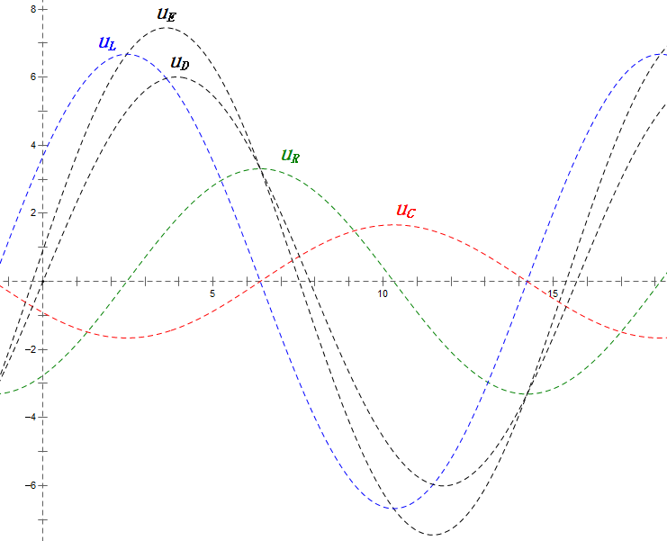
Analysis:
- Maximum current ≈ 1.57mA, safe for components.
- Phasor diagram forms a right trapezoid.
- At 2ω0, XL > XC → larger UL, smaller UC. Maximum uL and uE exceed power supply voltage, raising inductor damage concerns.
- uC lags uD by ≈150°; charging begins when uD drops to ≈half its maximum, ending when uR = uD = 0.
- Sine wave diagram segments represent half the time of Case 2.
- Equations uR = uE – uL and uC = uD – uE hold true at every moment.
