Confirm the Device and Package
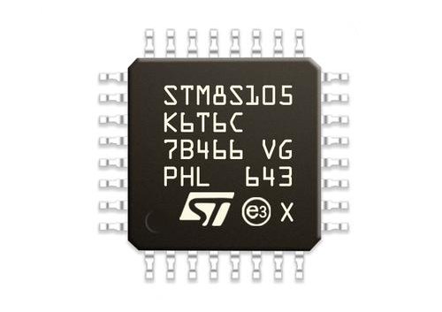
The STM8S105K6 is a 16 MHz, 8-bit STM8 microcontroller with 32 KB of program Flash, 2 KB of RAM and 1024 bytes of data EEPROM. Its peripherals include ADC1, UART2, SPI, I²C and timers. These capabilities can support a sensor board, but they do not establish how a particular board samples, calibrates or transmits measurements.
Record the complete device marking, package and board revision before identifying test points. ST’s STM8S105x4/6 datasheet, tables 1 and 5, distinguishes the package variants. The LQFP32 and UFQFPN32 columns share the pin numbers used below; the older SDIP32 package uses a different mapping. Confirm orientation and the package’s pin-1 indicator before tracing any net.
Map Reset, SWIM and Communication Signals
For LQFP32/UFQFPN32, NRST is pin 1, PD1/SWIM is pin 26, PD5/UART2_TX is pin 30 and PD6/UART2_RX is pin 31. PC1 is pin 18, while PC7/SPI_MISO is pin 24. Port-bit names run from 0 to 7; PC8 through PC11 are not valid STM8 port-bit names. Use the manufacturer’s table rather than copying a connector or pin list from another MCU.
Trace the actual board connections and check whether a pin is being used as GPIO or for an alternate function. Before connecting a supported programming tool, confirm ground, target supply reference, SWIM and reset wiring against the tool’s documentation. UART wiring identifies a possible communication path; it does not prove that a firmware-update protocol or an accessible bootloader is present.
Trace the ADC Sensor Signal Chain
The K6 device provides seven inputs to its 10-bit ADC1. For each sensor input, record the package pin, ADC channel, signal-conditioning circuit and relevant supply conditions. Include dividers, amplifiers, filters and protection components in the net map: the voltage at the MCU pin may differ substantially from the physical quantity being measured.
Check the datasheet’s input limits, source-impedance and acquisition requirements before choosing a test signal. AIN12 on PF4 has a specific limitation: it is not selectable in ADC scan mode or with the analog watchdog. Do not assume that every available analog input supports the same operating modes. Record raw ADC codes alongside the known input, channel configuration and sampling conditions, rather than presenting an unverified conversion formula as a recovered algorithm.
Separate Program Code from Calibration Data
The 32 KB program Flash occupies 0x008000–0x00FFFF, RAM occupies 0x000000–0x0007FF, and data EEPROM occupies 0x004000–0x0043FF. Record the address range and length of each available file. A raw binary needs an explicit load address; a program-memory image does not automatically include EEPROM contents or option-byte configuration.
Calibration coefficients may reside in EEPROM, program Flash, external memory or an update package. Establish their location and format from design records or reproducible analysis. Preserve units, scaling, byte order, version information and integrity checks where these are documented. Finding a recognizable string or a matching checksum alone does not demonstrate that a complete calibration algorithm has been recovered.
Preserve Contents Before Changing Protection
STM8 readout protection is configured through its ROP option byte. It should not be described using STM32-style Level 2 protection or STM32-specific option-register code. Readout protection also does not establish that an application uses XOR encryption: any application-specific encoding scheme needs its own evidence.
ST’s RM0016 reference manual, section 4.5.1, explains that removing readout protection automatically erases program Flash, the DATA area and option bytes. If original contents must be preserved, stop at an erase or unprotect prompt. Seek owner-supplied source code, production binaries, calibration records or verified backups before proceeding. Supported access must be authorized; recovery from a protected device cannot be assumed.
Build a Reproducible Measurement Record
On a suitable bench setup, compare known inputs with raw ADC readings and any reported output. Record the supply, clock configuration, firmware version, channel settings, settling time and test equipment. Where UART traffic is available, retain the original captures and distinguish observed frame behavior from an inferred protocol.
For an approved maintenance change, compare before-and-after behavior across the documented measurement range, startup conditions and fault handling. Keep the original files and hashes; matching hashes establish copy consistency, not firmware authenticity or correct sensor operation. This guide describes an assessment method, not a completed controller-fleet recovery, a validated protection bypass or a set of measured project results.
Decide What a Maintenance Plan Can Support
A sensor-board maintenance plan should identify which firmware, calibration data and hardware assumptions have been verified. If the original program is unavailable, a replacement design needs its own measurement requirements, interface specification and acceptance tests. Access to a binary alone does not establish the sensor’s transfer function, accuracy or environmental performance.
Report remaining gaps explicitly, including unknown coefficient formats, undocumented communication behavior and untested operating conditions. Use device-specific STM8 documentation for implementation. Register examples for unrelated DAC or RTC peripherals, and generic key-generation snippets, cannot stand in for a tested design on this device.
Discuss an STM8 board assessment:

Principal Engineer:
Dr. Billy Zheng
Well Done PCB Technology
billy@reversepcb.com
Emergency Support: +86-157-9847-6858