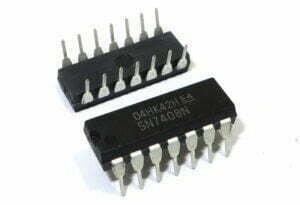
STM32F3 includes a series of 32-bit MCUs with high performance, real-time functionality, digital signal processing, low power consumption and low voltage operation, while maintaining high integration and ease of development. The unrivaled range of STM32 products is based on an industry-standard core and offers a wide range of tools and software options, making the range ideal for small projects to complete platforms.
Introduction to STM32F3
STM32F3 is the latest product launched by STmicroelectronics. It integrates a 32-bit ARM Cortex-M4 core with DSP and FPU instructions operating at 72 MHz, advanced analog peripherals, and embedded Flash and SRAM memory. Due to the integrated efficient power structure and multiple power consumption modes, STM32F3 reduces application-level power consumption and simplifies application design.
This series of MCUs also integrates a fast 12-bit 5 MSPS, precision 16-bit sigma-delta ADC, programmable gain amplifier (4 gain steps, 1% accuracy), fast 50 ns comparator and multi-function operating frequency of 144 MHz. Clock control unit.
Due to its real-time capabilities, digital signal processing, low power consumption and low voltage operation, the STM32F3 can effectively handle mixed signals in circuits such as three-phase motor controllers, biochemical and industrial sensors, and audio filters, and can be widely used in consumer, medical, Practical applications for portable fitness, system monitoring and measurement.
Features of STM32F3
- Ultra-fast comparator (25 ns)
- Operational amplifier with programmable gain
- 12-bit DAC
- Ultra-fast 12-bit ADC, 5 M samples per second per channel (five million samples per second), up to 18 M samples per second in alternating mode
- Precise 16-bit sigma-delta ADC (21 channels)
- Core Coupled Memory SRAM (Program Accelerator) is a memory architecture dedicated to improving the performance of time-critical programs, which can increase performance by 43%
- 144 MHz advanced 16-bit PWM timer (resolution < 7 ns) for control applications
- High-resolution timer (217 ps), self-compensating for power supply and temperature drift
- The flexible interconnect matrix enables autonomous communication between peripherals, saving CPU resources and power consumption.
STM32F3 Specifications
The STM32 F3 series includes devices with 64 to 256KB of on-chip Flash memory and 48KB of SRAM. Package options include WLCSP66 (less than 4.3 x 4.3 mm), LQFP48, LQFP64, LQFP100 and UFBGA100.
| Manufacturer | STMicroelectronics |
|---|---|
| Core | ARM Cortex M4F |
| Data Bus Width | 32 bit |
| I/O Count | 39 |
| Maximum Clock Frequency | 72 MHz |
| Flash Memory (Maximum) | 256 KB |
| Data RAM Size | 32 KB |
| On-chip ADC | Yes |
| Operating Supply Voltage | 1.65 V to 3.6 V, 2 V to 3.6 V, 2.2 V to 3.6 V |
| Operating Temperature Range | -40°C to +85°C |
| Package | LQFP-48, 64, 100 |
| Mounting Style | SMD/SMT |
STM32F3 Clock
STM32F3 uses 4 clock sources: LSE for embedded RTC; HSE for MCU operation; HSI for system clock; LSI for driving IWDG and RTC. Each clock source can be turned on or off individually when not in use to reduce power consumption.
HSE Clock
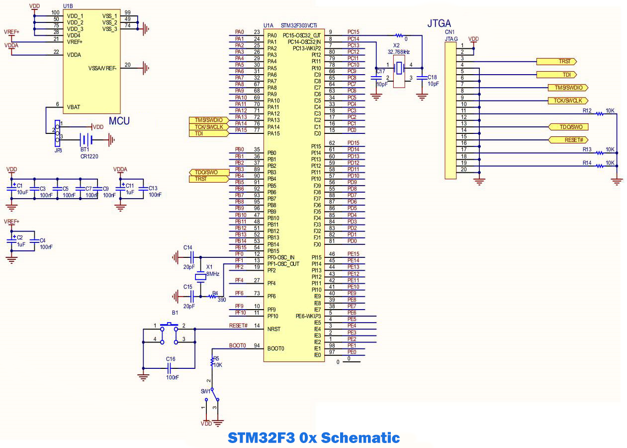
The high-speed external clock signal (HSE) OSC clock has 2 clock sources: HSE external crystal oscillator/ceramic resonator, HSE user external clock. When laying out the PCB, the resonator and load capacitance must be as close as possible to the oscillator pins to minimize output distortion and oscillation settling time. The load capacitance value must be adjusted appropriately according to the selected oscillator.
External crystal oscillator (HSE crystal oscillator)
The advantage of the 4-32MHz external oscillator is that it has very high accuracy. The HSERDY flag (RCC_CR) in the clock control register indicates whether the HSE oscillator is stable. This clock cannot be used until hardware sets this bit at startup. Interrupts can be generated if interrupts are enabled in the clock interrupt register (RCC_CIR). The HSE crystal oscillator can be turned on or off through the HSEON bit in the clock control register (RCC_CR).
External source (HSE bypass)
In this mode, an external clock source must be provided, with a maximum frequency not exceeding 32MHz. The OSC_IN pin must be driven using an external clock signal (square, sine or triangle wave) with a duty cycle of 40-60%, depending on the frequency, while the OSC_OUT pin can be used as a GPIO.
LSE Clock
The LSE crystal oscillator is a 32.768kHz low-speed external crystal oscillator or ceramic resonator. It can be used as the clock source of the real-time clock (RTC) to provide clock/calendar or other timing functions. It has the advantages of low power consumption and high accuracy.
The LSE crystal oscillator is turned on and off through the LSEON bit in the backup domain control register (RCC_BDCR). The crystal drive strength can be changed at runtime using the LSEDRV[1:0] bits in the Backup Domain Control Register (RCC_BDCR) to achieve the best balance between robustness, short startup time and low power consumption.
The LSERDY flag in the backup domain control register (RCC_BDCR) indicates whether the LSE crystal oscillator is stable. At startup, the LSE crystal oscillator output clock signal can be used only after the hardware sets this bit. Interrupts can be generated if interrupts are enabled in the clock interrupt register (RCC_CIR).
In this mode, an external clock source must be provided, with a maximum frequency not exceeding 1MHz. An external clock signal (square wave, sine wave or triangle wave) with a duty cycle of approximately 50% must be used to drive the OSC32_IN pin, while the OSC32_OUT pin can be used as a GPIO.
HSI Clock
The HSI clock signal is generated from the internal 8MHz RC oscillator and can be used directly as the system clock (SYSCLK) or as a PLL input. The advantage of the HSI RC oscillator is its lower cost (no external components required). In addition, its startup speed is faster than that of the HSE crystal oscillator block, but even after calibration, its frequency accuracy is not as good as that of an external crystal oscillator or ceramic resonator.
Because the production process is different, the RC oscillator frequencies of different chips are also different. ST performs factory calibration on each device to achieve an accuracy of 1% at TA = 25 ℃. In addition, the HSI clock can be connected to the MCO multiplexer. The clock can be connected to the input of Timer 16 in the F30x and to the input of Timer 14 in the F37x to allow the user to calibrate the oscillator.
LSI Clock
The low-speed internal RC clock (LSI RC) frequency is approximately 40kHz (between 30kHz and 60kHz). The LSI clock can be used as a low-power clock source to keep running in stop and standby modes to drive the independent watchdog (IWDG) and RTC. It can also be optionally provided to the RTC for automatic wake-up in stop/standby mode.
PCB Design of STM32F3
For technical reasons it is better to use a multi-layer printed circuit board (PCB) with one layer dedicated to ground (VSS) and another layer dedicated to VDD power supply. This provides good decoupling and shielding.
Component Location and Parameters
The initial layout of the PCB must have separate circuits with high current circuits, low voltage circuits, digital component circuits, and circuits separated based on the EMI characteristics of the circuit. This helps reduce cross-coupling that causes noise on the PCB. Refer to the table below for relevant component parameters.
| Components | Value | Count | Notes |
|---|---|---|---|
| MCU | STM32F303VCT6 | 1 | 100-pin package |
| Capacitor | 100nF | 4 | For STM32F303: 4 units For STM32F373/378: 3 units Ceramic Capacitors (Decoupling) |
| Capacitor | 4.7μF | 1 | Ceramic Capacitor (Decoupling) |
| Resistor | 390Ω | 1 | For HSE: Value depends on crystal characteristics. |
| Resistor | 0Ω | 1 | For LSE: Value depends on crystal characteristics. |
| Resistor | 10KΩ | 4 | For JTAG and boot mode pull-up and pull-down resistors. |
| Capacitor | 100nF | 3 | For RESET button, VDDA, and VREF+ (Ceramic Capacitors). |
| Capacitor | 1μF | 2 | For VDDA and VREF+. |
| Capacitor | 100nF | 3 | For VDDSDx and VREFSD+ (Ceramic Capacitors, only for STM32F37x). |
| Capacitor | 1μF | 3 | For VDDSDx and VREFSD+ (only for STM32F37x). |
| Capacitor | 10pF | 2 | For LSE: Value depends on crystal characteristics. |
| Capacitor | 20pF | 2 | For HSE: Value depends on crystal characteristics. |
| Crystal | 8MHz | 1 | For HSE |
| Crystal | 32kHz | 1 | For LSE |
| Embedded | 3V3 | 1 | If an external battery is not used in the application, it is recommended to connect VBAT externally to VDD. |
| Switch | - | 1 | For selecting the correct boot mode. |
| Button | B1 | 1 | Used as a reset button. |
| JTAG Connector | - | 1 | For MCU programming/debugging. |
Ground and Power Supply (VSS, VDD, VSSA, VDDA, VSSSD, VDDSD)
Each block (noise, bottom sensitive, digital, etc.) should be individually grounded, and all ground returns should be a single point. Rings must be avoided or have a minimum area. The power supply should be implemented close to the ground wire to minimize the area of the power supply loop. This is because the power loop behaves like an antenna, so it is the primary sender and receiver of EMI. All component-free PCB areas must be filled with additional ground to create shielding (especially when using single-layer PCBs).
Decoupling
All power and ground pins must be properly connected to the power supply. These connections, including pads, traces, and holes, should be as low-resistance as possible. Generally, this is achieved by widening trace widths, preferably using dedicated power planes in multilayer PCBs.
In addition, each power supply pair should be decoupled with a 100nF filter ceramic capacitor and connected between the power supply pins of the STM32F3xx device with a chemical capacitor of approximately 4.7μF. These capacitors need to be placed as close as possible next to or below the appropriate pins on the lower part of the PCB. Typical values are 10nF to 100nF, but the exact value depends on application needs.
Unused I/O
Usually an application will not use 100% of MCU resources. To increase EMC performance and avoid additional power consumption, unused clocks, counters or I/O should not be left floating and should be tied to fixed 0 or 1 logic levels. The method is to use external or internal pull-up or pull-down resistors on unused I/O pins; or use software to configure the GPIO into output mode. Features that are not used should be frozen or disabled, which is also their default value.
Different Types of STM32F3
The STM32F3 series MUCs include STM32F301, STM32F302, STM32F303 and other types. Not only do they integrate a variety of peripherals, but they also offer higher performance and analog capabilities to manage up to three FOC motor controls.
STM32F301
STM32F301 is a mixed-signal MCU that uses the ARM Cortex-M4 core (DSP, FPU) and runs at 72 MHz.
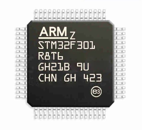
This series of MCUs has the following specifications:
- Up to 3 ultra-fast comparators (<30 ns)
- Operational amplifier (PGA) with programmable gain • 12-bit DAC
- Ultra-fast 12-bit ADC with 5M samples per second
- Fast motor control timer at 144 MHz (resolution < 7 ns)
- STM32F301 MCU operates from 2.0 to 3.6 V
- Memory capacities range from 32 to 64K bytes and packages are available from 32 to 64 pins
STM32F302
STM32F302 is a mixed-signal MCU that uses the ARM Cortex-M4 core (DSP, FPU) and runs at 72 MHz.
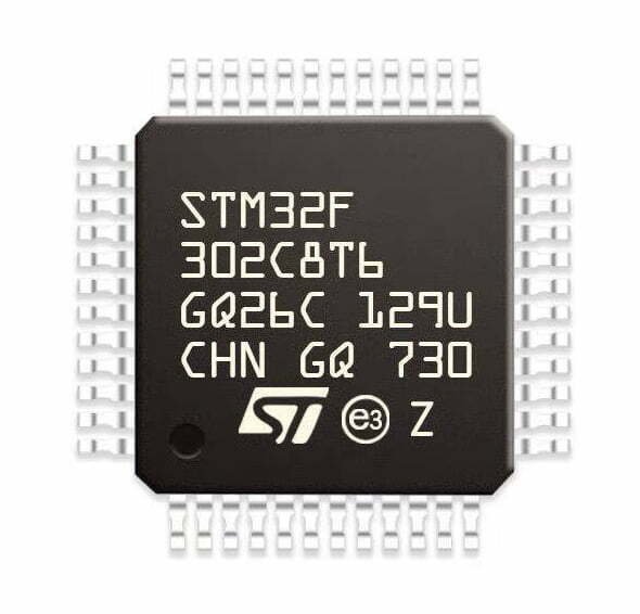
This series of MCUs has the following specifications:
- Up to 4 fast and ultra-fast comparators (<30 ns)
- Up to 2 operational amplifiers (PGA) with programmable gain
- 12-bit DAC
- Up to 2 ultra-fast 12-bit ADCs with 5M samples per second
- Fast motor control timer at 144 MHz (resolution < 7 ns)
- USB FS and CAN 2.0B communication interface
- STM32F302 MCU operates from 2.0 to 3.6 V
- Memory capacities range from 32 to 256K bytes and packages from 32 to 100 pins
- Temperature range is -40 to 85°C or -40 to 105°C (junction temperature is 125°C)
STM32F303
STM32F303 is a mixed-signal MCU that uses the ARM Cortex-M4 core (DSP, FPU) and runs at 72 MHz. This is a group of devices with excellent performance in the STM32F30x series of MCUs.
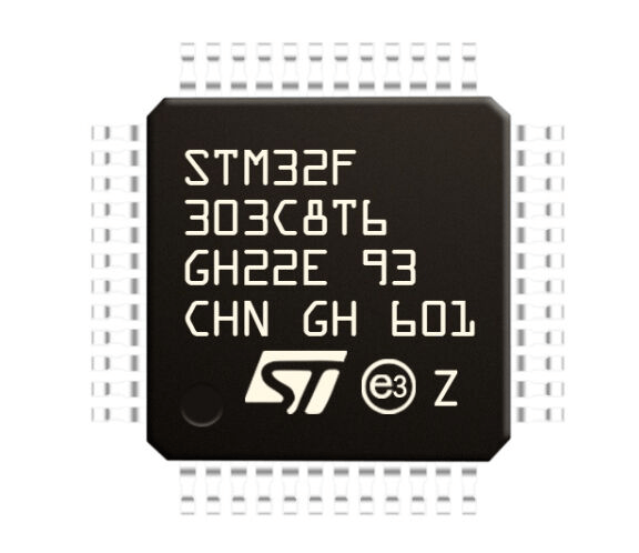
This series of microcontrollers has the following specifications:
- Up to 7 fast and ultra-fast comparators (<30 ns)
- Up to 4 operational amplifiers (PGA) with programmable gain
- Up to 2 12-bit DACs
- Up to 4 ultra-fast 12-bit ADCs at 5M samples per second
- Up to 3 fast motor control timers at 144 MHz (resolution < 7 ns)
- USB FS and CAN 2.0B communication interface
- Core-coupled memory SRAM (43% performance improvement compared to Flash execution)
- STM32F303 MCU operates from 2.0 to 3.6 V
- Memory capacities range from 32 to 256K bytes and packages from 32 to 100 pins
- Temperature range is -40 to 85°C or -40 to 105°C (junction temperature is 125°C)

