What Is a JFET?
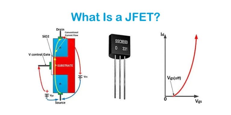
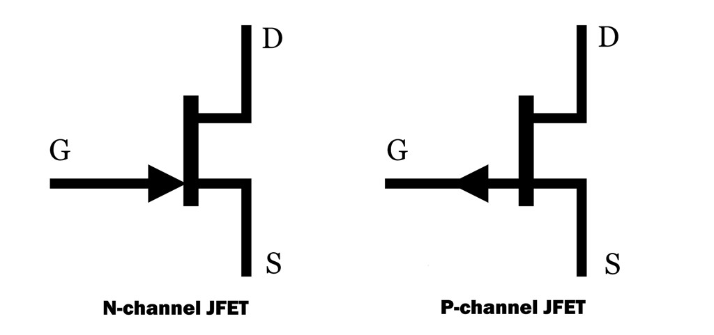
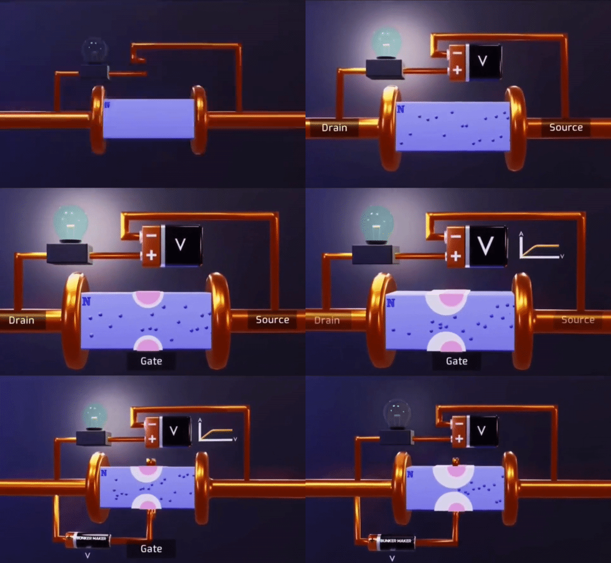
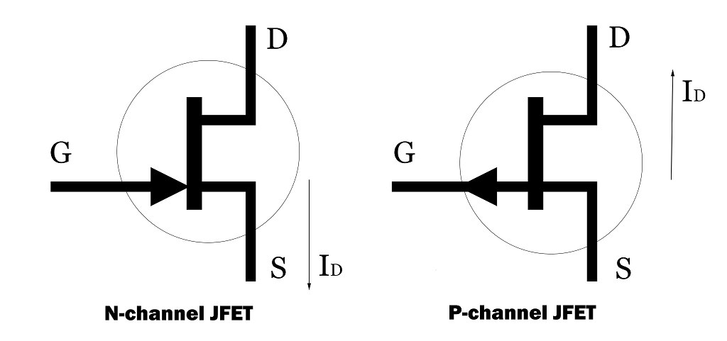
Junction Field Effect Transistor (JFET) is a three-terminal active device with amplification function, and is the simplest type of unipolar field effect transistor. It is composed of p-n junction gate (G), source (S) and drain (D), which can be divided into N channel or P channel, as shown in the following figure:
How JFETs Work?
We can’t study the relationship between JFET’s input voltage UGS and input current iG like BJT, because JFET has extremely high input impedance, and iG is approximately 0. Therefore, we can only study the relationship between the input voltage UGS and the output current iD, which is called the transfer characteristic; the relationship between the output voltage UDS and the output current iD is called the output characteristic. The figure below shows the curves of transfer characteristic and output characteristic:
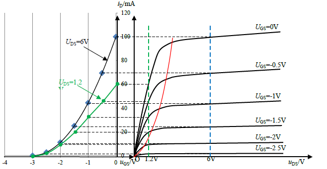
Actually, the transfer characteristic curve and the output characteristic curve are redundant. In other words, we can draw another graph from one graph. The method is also very simple. For example, we draw a vertical line at the position of UDS=6V in the right picture, which intersects with multiple curves, and the obtained points are drawn as the curve of the left picture (labeled UDS=6V). Another example is to select the position of UDS=1.2V, draw a vertical line, and you will get different transfer characteristic curves in the left picture (label UDS=1.2V green line).
How to judge the working status of JFET?
The working state of JFET is more complicated. In normal operation, it can work in cut-off region, variable resistance region and constant current region. In addition, it also has abnormal working conditions, such as the state where UGS is greater than 0V for N-channel JFETs.
Step 1: Identify the S source and D drain of the JFET
The S and D of the JFET in many circuits are not marked, so we need to learn to distinguish the S source and D drain of the JFET in the circuit.
The rules are as follows:
N-channel JFET, the current direction generated by the external power supply flows from D to S.
P-channel JFET, the direction of current generated by the external power supply is from S to D.
Step 2 : Judge the status of JFET
Once you have identified the pins (S source and D drain), you can easily judge the working state of the JFET according to the table below.
| N-channel JFET | UGS≤UGSOFF | UGS<UGSOFF≤0v | UGS>0V |
| Cut-off Area | UDS<UDS_DV, Variable Resistance Area | Abnormal state | |
| UDS>UDS_DV, Constant Current Zone | |||
| P-channel JFET | UGS≥UGSOFF | UGSOFF>UGS≥0v | UGS<0V |
| Cut-off Area | UDS>UDS_DV, Variable Resistance Area | Abnormal state | |
| UDS<UDS_DV, Constant Current Area |
Features of JFET
- JFET ability to operate in either the depletion mode or the enhancement mode:
– In the depletion mode, the JFET is normally ON, and the current flows through the channel when no voltage is applied to the gate terminal.
– In the enhancement mode, the JFET is normally OFF, and the current flow through the channel is controlled by the voltage applied to the gate terminal.
- The JFET has a high input impedance, which means it can accept a wide range of input signals without affecting the performance of the circuit.
- The JFET has a low output impedance, which means it can drive low impedance loads with minimal signal degradation.
- JFETs can be used as voltage-controlled resistors, where the resistance of the channel can be controlled by the voltage applied to the gate terminal.

