Designing a printed circuit board (PCB) schematic is a critical step in the electronics development process. It forms the blueprints for fabricating the PCB, ensuring that all components, connections, and traces are accurately represented. Whether you’re developing a simple hobby project or a complex system, creating a well-structured and efficient schematic is essential. This guide will walk you through the process, from understanding the requirements to finalizing the design and documentation. By following these steps, you can create a PCB schematic that meets your project’s needs and is ready for manufacturing.
Understanding the Requirements
Before diving into the design process, it’s crucial to have a clear understanding of your project’s requirements. This includes defining the electronic functions, power requirements, signal specifications, and physical constraints such as board size, component density, and cost considerations.
- Define the Project Goals: Identify the purpose of your PCB, whether it’s for a communication system, motor control, or signal processing. This will shape the circuit topology and component selection.
- Consider Constraints: Analyze factors like available space, budget, and environmental conditions (e.g., temperature or humidity). These constraints will influence your design decisions.
- Involve Stakeholders: Collaborate with team members or clients to ensure everyone has a shared understanding of the project requirements. Miscommunication can lead to costly redesigns.
Taking the time to thoroughly understand your requirements will help you avoid errors and ensure the final design meets all necessary criteria.
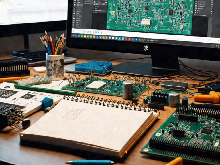
Selecting the Right Tools and Software
The tools you use will significantly impact the efficiency and accuracy of your schematic design process. There are several software options available, each with unique features and interfaces.
- Choose the Right Software: Select a PCB design tool that aligns with your skill level and project complexity. Popular options include KiCad (open-source), Altium Designer, and EagleCAD.
- Consider Licensing: Ensure the software is compatible with your operating system and check licensing terms to avoid unexpected costs.
- Familiarize Yourself: Spend time learning the tool’s interface and features. For example, KiCad is free but may have a steep learning curve for beginners.
Investing time in selecting the right software will pay off in the long run, as it will streamline your design process and reduce the chances of errors.
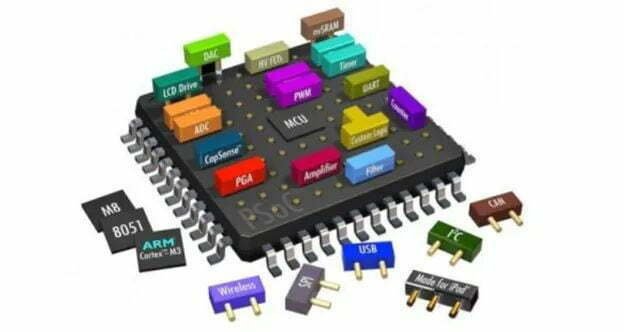
Designing the Circuit Topology
The circuit topology is the foundation of your PCB schematic. It involves defining the electrical connections and layout for all components, ensuring they function as intended.
- Start with Components: Begin by placing resistors, capacitors, and other passive components on the board. Consider their placement to optimize signal routing.
- Analog vs. Digital Circuits: Choose the right topology for your application. Analog circuits are ideal for applications like filtering and amplification, while digital circuits are better suited for logic operations.
- Mixed-Signal Designs: If your project requires both analog and digital components, ensure they are properly integrated and isolated to prevent interference.
A well-thought-out circuit topology will ensure that your PCB operates reliably and efficiently.
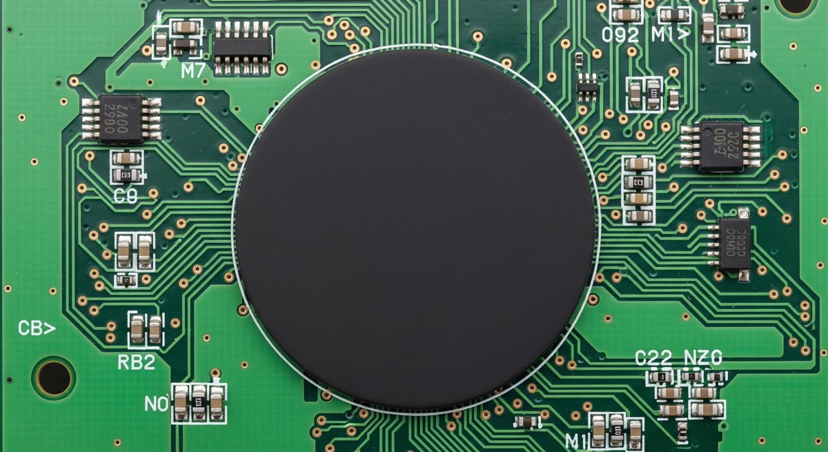
Placing Components on the Board
After defining the circuit topology, it’s time to place the components on the PCB. This step involves mapping the circuit design onto the physical layout of the board.
- Place Components Strategically: Position components such as resistors, capacitors, and integrated circuits in a way that minimizes trace length and avoids overcrowding.
- Consider Footprints: Ensure that the component footprints match the available pads on the PCB. Misaligned footprints can lead to assembly errors.
- Follow Best Practices: Keep traces short to reduce resistance and avoid placing components too close together to prevent signal interference.
Precision is key when placing components, as even small errors can compromise the functionality of your PCB.
Routing Signals for Proper Communication
Signal routing is the process of connecting components and traces to ensure proper communication. This step is critical for ensuring the PCB operates as intended.
- Plan Signal Paths: Define the paths for power, ground, and signal traces. Use the PCB layout tool to draw lines between components.
- Optimize Routing: Use techniques like keep-out areas and staggered routing to minimize signal crosstalk and improve board density.
- Power and Ground Routing: Ensure that power and ground traces are routed appropriately to provide stable power supply to all components.
Carefully routing signals will ensure that all parts of your circuit can communicate effectively.
Creating a Bill of Materials
A Bill of Materials (BOM) is a critical document that lists all the components required to build the PCB. It ensures that everyone involved in the project has a clear understanding of the parts needed.
- List Components: Include each component’s part number, value, and quantity. Use standardized library symbols to represent each part.
- Reference Descriptions: Add brief descriptions or reference designs to clarify the purpose of each component.
- Verify Accuracy: Cross-check the BOM with the circuit design to ensure all components are accounted for.
A complete and accurate BOM will facilitate smooth manufacturing and assembly processes.
Adding Power and Ground Traces
Power and ground traces are essential for providing stable power to all components on the PCB. Properly routing these traces ensures the board operates reliably.
- Power Supply Routing: Connect the power supply to the board’s power and ground pads. Ensure the traces are wide enough to handle the required current.
- Ground Routing: Similarly, route the ground traces to ensure all components are grounded properly.
- Decoupling Capacitors: Add decoupling capacitors where necessary to filter noise and stabilize the power supply.
Adding robust power and ground traces is a key step in ensuring the PCB’s functionality.
Testing the Schematic with Simulations
Before finalizing the design, it’s essential to test the schematic using simulation tools. This step helps identify potential issues early in the design process.
- Simulate Signals: Use simulation tools to check for voltage drops, signal interference, and timing violations.
- Check Thermal and Mechanical Stress: Simulate the board’s thermal expansion and mechanical stress to ensure it can withstand real-world conditions.
- Power Integrity: Verify that the power and ground traces can handle the current and voltage requirements.
Testing the schematic with simulations ensures that the design is robust and reliable.
Documentation for Clarity and Collaboration
Finally, create comprehensive documentation to support the PCB design. This ensures that others can understand and build upon your work.
- Component and Symbol Documentation: Include detailed information about each component, such as its datasheet and pin configuration.
- Layout and Dimension Information: Provide dimensions, keep-out areas, and other relevant layout details.
- Version Control: Maintain a history of design changes to track the evolution of the PCB.
Clear documentation facilitates collaboration and minimizes confusion during the manufacturing and assembly phases.
Conclusion
Creating a PCB schematic is a complex but rewarding process that requires careful planning, precision, and attention to detail. By following the steps outlined in this guide, you can design a PCB that meets your project’s requirements and is ready for manufacturing. Whether you’re a seasoned engineer or a hobbyist, understanding the principles of PCB design will help you create more efficient and reliable circuits. With practice and experimentation, you can master the art of PCB schematic creation. Happy designing!