Automatisierung des elektronischen Designs (EDA) ist die Kategorie von Software-Tools, die Ingenieure zum Entwerfen, Simulieren und Verifizieren elektronischer Systeme verwenden, bevor eine einzelne Platine hergestellt wird. Wenn Sie denken, dass EDA nur „schematische Erfassung“ bedeutet, fehlt Ihnen das meiste, was moderne EDA-Toolchains tatsächlich tun. In diesem Artikel wird erläutert, was Tools für die elektronische Design-Automatisierung tun, wie sie sich voneinander unterscheiden und worauf sie bei der Auswahl einer EDA-Plattform für PCB-Arbeiten achten müssen.
Was die elektronische Designautomatisierung tatsächlich abdeckt
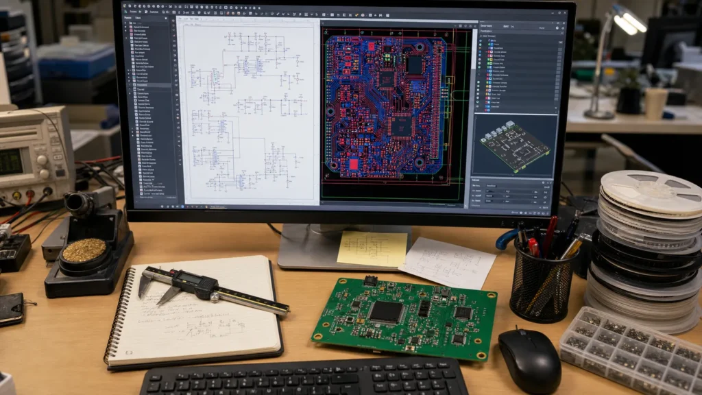
Zumindest ein Automatisierung des elektronischen Designs Toolchain übernimmt vier Stufen:
Schematische Erfassung: Zeichnen der logischen Schaltung. Hier platzieren Sie Symbole, Kabelverbindungen und weisen Komponentenwerte zu. Ein gutes Schema-Tool verwaltet auch hierarchische Blätter, Entwurfsregelprüfungen (DRC) und elektrische Regelprüfungen (ERC).
PCB-Layout: Übersetzen des Schaltplans in eine physische Platine. Der PCB-Editor platziert Footprints, leitet Kupferspuren, definiert Ebenenebenen und wendet Entwurfsregeln für die Freigabe, Impedanz und Herstellbarkeit an.
Simulation und Analyse: SPICE-Simulation für analoge Schaltungen, Signalintegritätsanalyse für High-Speed-Digital-, Thermal-Simulations- und PDN-Analyse (Power Distribution Network). Diese laufen innerhalb oder neben dem EDA-Tool.
Produktionsleistung: Generieren von Gerber-Dateien, Bohrdateien, Pick-and-Place-Daten und Montagezeichnungen. Fehler in diesem Stadium führen zu Fabrication Rejects.
Weitere Informationen zu schematischen Best Practices finden Sie unter ReversePCBS PCB Schaltplan-Designhandbuchein
Wichtige EDA-Plattformen für PCB-Design
Die EDA-Landschaft teilt sich ungefähr in drei Ebenen auf, und die Auswahl der falschen für Ihr Projekt verursacht echte Schmerzen:
| Stufe | Werkzeuge | am besten für | Einschränkungen |
|---|---|---|---|
| Open-Source / Kostenlos | KiCad, Easyeda, LibrePCB | Hobbyprojekte, offene Hardware, 2-6-Schicht-Boards | Begrenzte fortgeschrittene Simulation, weniger robuste Bibliotheksverwaltung |
| Mittelklasse Profi | Altium Designer, Orcad, Pads | Professionelle 4-16-Schicht-Boards, High-Speed-Design, Team-Workflows | Abonnementkosten, steile Lernkurve |
| Unternehmen / RF-spezialisiert | Cadence Allegro, Mentor Xpedition, Anzeigen | Komplexe Mehrschicht-, HF/Mikrowelle, HDI, Starr-Flex | Sehr hohe Kosten, erfordert engagiertes CAD-Support-Personal |
KiCad hat die Lücke mit Werkzeugen der Mittelklasse für viele Designs geschlossen. Es ist jetzt eine praktikable professionelle Wahl für Boards bis zu 8 Schichten, vorausgesetzt, Ihr Team ist mit dem Bibliotheks-Workflow vertraut. Wenn Sie eine High-Speed-Digitalplatine mit DDR-Speicher oder Differenzpaaren mit mehreren GHz entwerfen, werden die Signalintegritätstools von Altium oder Cadence-Level schwerer zu ersetzen.
Der Schema-zu-PCB-Workflow in der Praxis
So sieht der EDA-Workflow für ein typisches PCB-Projekt aus:
Erstellen Sie den Schaltplan. Platzieren Sie Symbole, Drahtnetze, weisen Sie Footprints zu und führen Sie den ERC aus, um nicht verbundene Pins oder widersprüchliche Ausgänge zu fangen.
Generieren Sie die Netzliste. Die Netzliste ist eine maschinenlesbare Liste aller Komponenten und Verbindungen. Das PCB-Layout-Tool importiert es.
Komponenten platzieren. Positionieren Sie Fußspuren auf der Platinenumrisse. Gruppieren Sie verwandte Teile, richten Sie die Anschlüsse korrekt aus und lassen Sie Platz für die Befestigung von Löchern und Haltezonen.
Spuren verlegen. Verbinden Sie die Pads gemäß der Netzliste unter Beachtung der Freigaberegeln, der Spurbreitenanforderungen und der Impedanzziele. Moderne EDA-Tools umfassen Auto-Routing, aber kritische Netze sollten immer hand-routed werden.
DRK ausführen. Der Entwurfsregelprüfer überprüft, ob kein Trace die Freigabe verletzt, kein Pad eine Verbindung verpasst und jedes Netz vollständig geroutet wird. Das Bestehen der DRK ist die Mindestanforderung, bevor ein Board zur Fabrication geschickt wird.
Fertigungsdateien generieren. Exportieren Sie Gerbers, NC-Bohrdateien, Stücklisten und Baugruppenzeichnungen. Überprüfen Sie den Gerber-Viewer – Fehler in diesem Stadium sind teuer.
Wenn Sie sich in Altium speziell von Schaltplan auf Leiterplatte bewegen, Diese Schritt-für-Schritt-Anleitung Geht durch den gesamten Prozess.
Worauf Sie bei der Auswahl eines EDA-Tools achten sollten
Konzentrieren Sie sich auf das, was Ihr Projekt tatsächlich beeinflusst, nicht auf das Marketing von Features:
Bibliotheksqualität und -verwaltung: Wird das Tool mit verifizierten Footprints für die Komponenten geliefert, die Sie tatsächlich verwenden, oder verbringen Sie Stunden damit, Symbole aus Datenblättern zu erstellen? Eine schwache Bibliothek verschwendet mehr Zeit als jede fehlende Simulationsfunktion.
Entwurfsregelfunktionen: Können Sie Regeln nach Netzklasse, Differenzpaar und Region definieren? Wenn Sie eine kontrollierte Impedanz benötigen, berechnet das Werkzeug die Spurengeometrie aus Ihrem Stackup?
Zusammenarbeit: Können mehrere Ingenieure am selben Projekt arbeiten? Unterstützt es die Versionskontrolle? Die Git-Integration wird in modernen EDA-Tools zunehmend Standard.
Fertigungsleistungszuverlässigkeit: Stimmen die Gerber-Exporte mit dem Board überein? Einige Werkzeuge wenden während der Ausgabe stillschweigend Designregelkorrekturen an, die das Board ändern. Überprüfen Sie jedes Mal in einem Gerber-Viewer.
Simulationsintegration: Wenn Sie sich auf SPICE-Simulation verlassen, integriert das Tool sie nativ oder müssen Sie Netzlisten in einen externen Simulator exportieren?
Häufige EDA-Fehler, die die Herstellung erreichen
Ungerestete Netze, die Demokratische Republik Kongo überschreiten: Einige Tools ermöglichen es nicht gerouteten Netzen, die DRC zu übergeben, wenn sie als „No-Connect“ gekennzeichnet sind. Überprüfen Sie jedes Netz visuell oder mit einem Konnektivitätsbericht.
Footprint Pin 1 Nichtübereinstimmung: Das schematische Symbol und der Leiterplatten-Fußabdruck sind in der Ausrichtung von Pin 1 nicht einverstanden. Dies ist die häufigste Ursache für Ausfälle von First-Revision-Boards. Überprüfen Sie auf jedem IC-Fußabdruck immer die Pin-1-Anzeige.
Überlappende Pads für Siebdruck: Siebdruck auf Kupferpads verhindert Löten. Die meisten Werkzeuge haben eine Siebdruck-zu-Pad-Clearance-Regel – aktivieren Sie sie.
Unübertroffene Impedanz: Die Trace-Geometrie im Layout erzeugt nicht die Zielimpedanz, da das Stackup im Werkzeug falsch definiert wurde. Überprüfen Sie die Impedanz mit dem Verarbeiters Ist-Stapelup, nicht das Werkzeugs Standard.
Häufig gestellte Fragen
Was ist die elektronische Design-Automatisierung?
Electronic Design Automation (EDA) ist eine Kategorie von Software zur Entwicklung elektronischer Systeme, einschließlich schematischer Erfassung, Leiterplattenlayout, Schaltungssimulation und Herstellungsdateigenerierung. EDA-Tools sind für die moderne Leiterplattenentwicklung unerlässlich.
Ist KiCad gut genug für professionelles PCB-Design?
Ja, KiCad ist jetzt in der Lage, professionelles Leiterplattendesign für Boards bis zu 8 Schichten zu erstellen. Es unterstützt das Differential-Paar-Routing, die Längenabstimmung und die 3D-Visualisierung. Für sehr schnelle Designs, die eine fortschrittliche Signalintegritätssimulation erfordern, bieten Altium- oder Cadence-Tools eine tiefere Analyse.
Was ist der Unterschied zwischen schematischer Aufnahme und PCB-Layout?
Schematische Erfassung ist die logische Entwurfsphase, in der Sie Komponentenverbindungen und Schaltungsfunktion definieren. Das PCB-Layout ist die physikalische Entwurfsphase, in der Sie Komponenten platzieren, Kupferspuren verlegen und die Platine für die Herstellung vorbereiten.
Benötige ich eine Simulation in meinem EDA-Tool?
Bei einfachen Digitalboards ist die Simulation optional. Für analoge Schaltungen, Netzteile oder digitale Hochgeschwindigkeitsdesigns fangen die SPICE-Simulation und die Signalintegritätsanalyse Probleme vor der Herstellung und Speichern von Revisionsdrehungen.
Welche Dateien generiert ein EDA-Tool für die Herstellung?
Zu den Standard-Herstellungsausgaben gehören Gerber-Dateien (RS-274X oder X2-Format) für jede Kupferschicht, Lötmaske und Siebdruck; NC-Bohrdateien; Pick-and-Place-Dateien für die automatische Montage; und eine Stückliste (BOM).