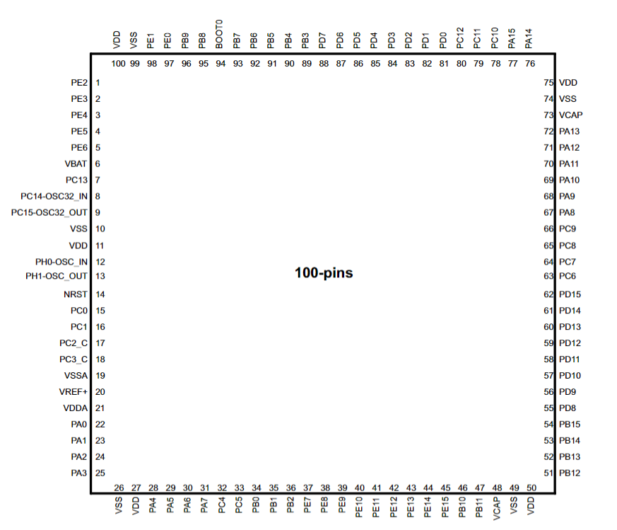
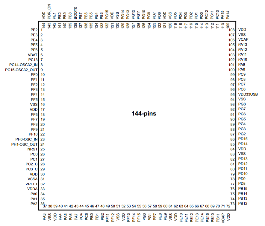
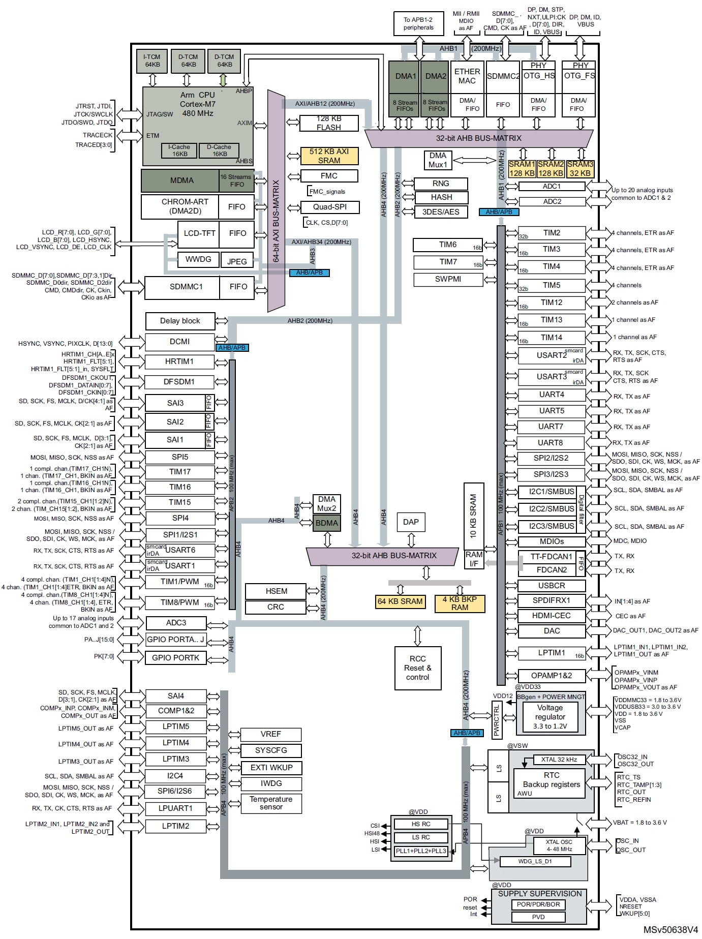
STM32H750VBT6 is a high-performance microcontroller launched by STMicroelectronics, which has excellent functions and a wide range of applications. In this article, we’ll introduce the features, specifications, application scenarios of STM32H750VBT6, and provide pin diagrams and block diagram for engineers.
STM32H750VBT6 Introduction
The STM32H750VBT6 device is based on a high-performance Arm Cortex-M7 32-bit RISC core, with a maximum operating frequency of 480MHz. The Cortex-M7 core features a floating-point unit (FPU) that supports both double-precision (IEEE754-compliant) and single-precision data processing instructions and data types.
The STM32H750VBT6 device supports a full set of DSP instructions and a Memory Protection Unit (MPU) to enhance application security. Additionally, this device includes high-speed embedded memory with 128KB of flash memory, up to 1MB of RAM (including 192KB of TCM RAM, up to 864KB of user SRAM, and 4KB of backup SRAM), as well as various enhanced I/O and peripheral memory access capabilities connected to the APB bus, AHB bus, 2×32-bit multi-AHB bus matrix, and internal and external multi-layer AXI interconnects.
STM32H750VBT6 Specification
| Property | Value |
|---|---|
| Manufacturer | STMicroelectronics |
| Package Style | LQFP-100, LQFP-144, LQFP-176 |
| Program Memory Size | 128KB |
| Data Bus Width | 32-bit |
| ADC Resolution | 3x 16-bit |
| Max Clock Frequency | 480MHz |
| I/O Pin Count | 82 |
| Data RAM Size | 1MB |
| Min Supply Voltage | 1.71V |
| Max Supply Voltage | 3.6V |
| Min Operating Temp | -40°C |
| Max Operating Temp | +85°C |
| DAC Resolution | 12-bit |
| Data RAM Type | Internal Memory |
| I/O Voltage | 1.62V to 3.6V |
| Interface Types | CAN, I2C, SAI, SDI, SPI, USART, USB |
| ADC Channel Count | 36 |
| Program Memory Type | Flash |
| Watchdog Timer | Windowed Watchdog Timer |
| Unit Weight | 11g |
STM32H750VBT6 Pin Configuration
STM32H750VBT6 Features
Core
- 32-bit Arm Cortex-M7 core with double-precision FPU and L1 cache: 16Kbytes data and 16Kbytes instruction cache; up to 400MHz frequency, MPU, 856DMIPS/2.14DMIPS/MHz (Dhrystone 2.1), and DSP instructions.
Memory
- Dual-mode Quad-SPI memory interface with up to 133MHz operating frequency.
- Flexible external memory controller with up to 32-bit data bus: SRAM, PSRAM, NOR Flash up to 133MHz in synchronous mode, SDRAM/LPSDR SDRAM, 8/16-bit NAND Flash.
Security
- ROP, PC-ROP, Secure Firmware Upgrade support, active tamper, Secure Access Mode.
General I/O
- Up to 168 I/O ports with interrupt capability.
Reset and Power Management
- 3 independent power domains with individual clock gating/control.
- 1.62V to 3.6V application supply and I/O voltage.
- POR, PDR, PVD, and BOR.
- Embedded USB power supply for internal PHY via 3.3V internal regulator.
- Embedded regulator (LDO) with configurable and scalable output for digital circuits.
- Voltage scaling in run and stop modes (5 configurable ranges).
- Backup regulator (~0.9V).
- Voltage reference for analog peripherals/VREF+.
- Low power modes: Sleep, Stop, Standby, and VBAT for battery charging support.
Low Power
- Very low total current consumption down to 4µA.
Clock Management
- Internal oscillators: 64MHz HSI, 48MHz HSI48, 4MHz CSI, 32kHz LSI.
- External oscillators: 4-48MHz HSE, 32.768kHz LSE.
- 3 PLLs with fractional mode.
Interconnect Matrix
- 3 bus matrices (1 AXI and 2 AHB).
- Bridges (5 AHB2-APB, 2 AXI2-AHB).
DMA Controllers
- 4 DMA controllers offloading CPU.
- 1 High-Speed Master Direct Memory Access controller (MDMA) with linked list support.
- 2 Dual-port DMAs with FIFOs.
- 1 Basic DMA with request router.
Analog Peripherals
- 3 ADCs, up to 16-bit resolution (up to 36 channels at 12-bit, 4.5MSPS).
- 1 Temperature sensor.
- 2 12-bit D/A converters (1MHz).
- 2 ultra-low-power comparators.
- 2 operational amplifiers (8MHz bandwidth).
- 1 digital filter for sigma-delta modulation (DFSDM) with up to 8 channels and 4 filters.
Graphics
- LCD-TFT controller with up to XGA resolution.
- Chrom-ART graphic hardware accelerator (DMA2D) to reduce CPU load.
- Hardware JPEG codec.
Timers and Watchdogs
- 1 High-resolution timer (2.5ns max resolution).
- 2 32-bit timers with up to 4 I2C/OC/PWM or pulse counters and quadrature (incremental) encoder inputs (up to 200MHz).
- 2 16-bit advanced motor control timers (up to 200MHz).
- 10 16-bit general-purpose timers (up to 200MHz).
- 5 16-bit low-power timers (up to 200MHz).
- 2 watchdogs (independent and window).
- 1 SysTick timer.
- RTC with sub-second precision and hardware calendar.
Encryption Acceleration
- AES 128/192/256, TDES.
- Hash (MD5, SHA-1, SHA-2), HMAC.
- True random number generator.
Debugging
- SWD and JTAG interfaces.
- Kilobyte-level embedded trace buffer.
STM32H750VBT6 Application
- Motor control and application management.
- Medical equipment.
- Industrial applications: PLC, inverters, circuit breakers.
- Printers and scanners.
- Alarm systems, video intercoms, and HVAC.
- Home audio devices.
- Mobile applications, IoT.
- Wearable devices: smartwatches.
STM32H750 Series ICs Unlock
- STM32H750VBT6
- STM32H750ZBT6
- STM32H750IBT6
- STM32H750XBH6
- STM32H750IBK6
Summary
In summary, the STM32H750VBT6 device is based on a high-performance Arm Cortex-M7 32-bit RISC core with a maximum clock frequency of 480MHz. The device supports full DSP instructions and a Memory Protection Unit (MPU) for enhanced application security. It features high-speed embedded memory with 128KB of flash and up to 1MB of RAM. With its wide range of capabilities, the STM32H750VBT6 is a popular choice across various industries.

