When designing printed circuit boards, you need to take into account how each layer of the board is going to affect the others. If you are designing a double-sided board, for example, it’s important to know which layers will be above or below one another so that you can make adjustments in your design accordingly.
This guide will help you understand what pcb stackup is, stackup designing rules and what sort of effects different layers have on the final product.
What is PCB Stackup?
Printed circuit board stackup is the layer arrangement of different materials in a printed circuit board (PCB). A typical printed circuit board stackup will consist of a copper layer, an insulation layer, a ground plane, and a signal layer. A PCB stackup has an effect on several properties of a printed circuit board including thermal performance, electromagnetic interference (EMI) performance, stress and strain response, and signal integrity.

Copper Layers
There are two types of copper layers, inner and outer. Inner copper layers are used to connect components together and outer copper layers are used for connections to external devices. The thickness of the copper layers is also important. The thickness should be 1 oz for inner layers and 2 oz for outer layers. Thinner copper may affect the performance of the circuit and be difficult to route. Thicker copper is more robust, but it also increases the cost of the board. The copper thickness should be selected based on the design requirements. For example, the thickness of the copper should be at least 0.01 mm wider than the width of the largest trace.
Signal Layers
Signal layers are used to carry high-speed digital signals such as data and clock signals. The two most common types of signal layers are single-ended and differential. Single-ended layers are used to carry a single signal. There is no ground reference, so the signal is vulnerable to noise. Differential layers are used to carry multiple signals with a ground reference. This is the most common type of layer and is ideal for RF circuits and high-speed communications. The thickness of the signal layers should be 0.5 oz or 1 oz. The thickness of the layer is determined by the width of the traces. The traces should be at least 0.004 mm wider than the trace width.
Insulating Layers
The insulating layers are used to isolate copper layers and prevent electrical short circuits. The two most common types of insulating layers are FR-4 epoxy and glass epoxy. FR-4 epoxy – FR-4 epoxy is a high-quality material that has excellent properties for use in PCBs including excellent thermal and mechanical properties. This is the most commonly used insulating material. Glass epoxy – Glass epoxy is a very high-quality insulating material. It is commonly used for high-end boards. Glass epoxy is more expensive than FR-4 epoxy, but it may be worth the cost for critical boards. The thickness of the insulating layers should be 1.5 mm. The thickness of the layer is determined by the width of the traces. The traces should be at least 0.005 mm wider than the trace width.
Ground Plane
An digital circuit’s ground plane shields it from electromagnetic interference, while also functioning as a return path for current. The ground plane should be 0.25 mm thick. The ground plane layer should be 0.005 mm wider than the trace width. A copper-nickel combination is preferable to a copper-only ground plane layer due to its shielding capability, although it is more costly and less conductive. A single layer of copper is less conductive and more susceptible to corrosion, but it is cheaper and easier to obtain.
Recommended PCB Stackup
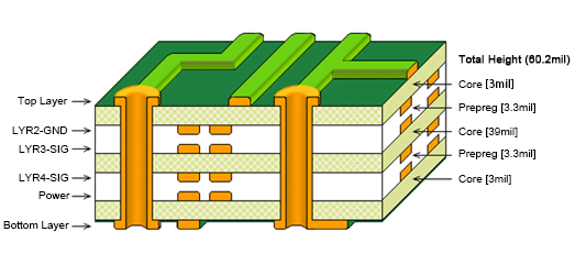
4 layer PCB stackup
The recommended 4 layer printed circuit board stackup below is based on industry experience and extensive research. This stackup is general enough to be used with multiple types of PCBs.

Top copper layer – Copper thickness: 1 oz, Solder mask material: FR-4, Nickel thickness: 1 oz or 2 oz;
Bottom copper layer – Copper thickness: 1 oz, Solder mask material: FR-4, Nickel thickness: 1 oz or 2 oz;
Insulation layer – 1.5 mm polyimide, Dielectric strength: 3000 V/mil;
Ground plane – 0.25 mm copper, Dielectric strength: 3000 V/mil.
6 layer PCB stackup
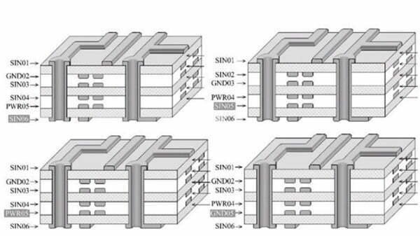
For the design with high chip density and high clock frequency, the design of 6-layer board should be considered. The recommended 6 layer pcb stackup method is shown in the following figure:

This stacking method can achieve better signal integrity, the signal layer is adjacent to the ground layer, the power layer and the ground layer are paired, the impedance of each trace layer can be well controlled, and both ground layers are well absorption magnetic field lines. And in the case of complete power supply and ground layer, it can provide a better return path for each signal layer.
8 Layer PCB Stackup
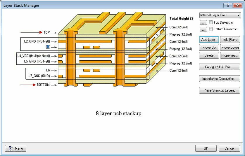
8-layer PCB boards are typically used in high-speed, high-performance systems. Some of these layers are used for power or ground planes, which are usually solid planes without divisions. This method uses a multi-layer ground reference plane, which has a very good ability to minimize the amount and effects of EMI.

The 8-layer structure is as follows:
Top layer – Signal 1: component surface, microstrip routing layer, good routing layer;
2nd Layer – Ground Plane: better electromagnetic wave absorption ability;
3rd Layer – Signal 2: Stripline routing layer, good routing layer;
4th Layer – Power Layer: constitutes excellent electromagnetic absorption with the underlying layers;
5rd Layer – Ground Plane;
6th Layer – Signal 3: Stripline routing layer, good routing layer;
7th Layer – Ground Plane: better electromagnetic wave absorption ability;
8th Layer – Signal 4: microstrip routing layer, good routing layer.
PCB Stackup Designing Rules
PCB stackup design is related to the requirements of circuit function, signal integrity, EMI, EMC, manufacturing cost, etc. Based on this, we have summarized these designing rules for your reference.
1. Using even-numbered layer structure
Our circuit design experience in the past suggests that the stack-up design is almost always an even-numbered layer structure, not an odd-numbered layer.
- Saving Cost
The processing cost of odd-layer PCBs is significantly higher than even-layer PCBs. Because the odd-numbered circuit board needs to add a laminated core layer on the basis of the core layer structure process.
- Avoid circuit board bending
An unusual lamination tension can result in an board bending. As the board thickness increases, so does the risk of bending. An odd-numbered circuit board is easy to bend, while an even-layered pcb can avoids bending.
2. Determining routing and vias
The wiring directions on the same signal layer should be consistent and orthogonal to those on adjacent signal layers. For example, the wiring direction on one signal layer might be set to the “Y-axis” direction, and the wiring direction on an adjacent signal layer might be set to the “X-axis” direction.
3. Choosing the layer arrangement
- It is important to establish proper layer positioning when using microstrip technology.
- Route high-speed signals on minimum-thickness microstrips, and place signal layers next to power layers for strong coupling.
- The power and ground layers should be spaced as close as possible.
- It is important to keep signal layers separate.
4. Select Short Signal Traces
The top and bottom layers of a multi-layer PCB are usually used to position components and a small number of signal traces. These signal traces should not be too long to reduce the direct radiation generated by them.
5. decoupling capacitors
When designing a PCB, it is important to use decoupling capacitors to ensure proper power delivery. Only the top and bottom planes should serve as locations for decoupling capacitors. The efficiency of these capacitors is largely dependent on the quality of the associated traces, pads, and vias. To guarantee proper functionality, the wires should be as short as possible and the vias should be as close as possible.
Material Options and Thickness for PCB Stackup
As introduction above, we know there’re three major components make up a PCB stackup: copper, insulation, and ground plane. The choice of material and thickness for each layer affects the performance characteristics of the final product.
Copper layers– There are many different types of copper available. Each type has a different melting temperature, electrical conductivity, and thermal expansion rate. The choice of copper is usually determined by the design requirements.
Always keep in mind that the thicker the copper layers, the more robust the overall design will be. But thicker copper layers will add to the cost of the board.
Insulation layers– The most common PCB insulating materials are FR-4 epoxy, glass epoxy, and parylene-coated materials. The selection of each type is determined by the application environment.
The insulation layer should be as thick as possible for EMI shielding and for increasing the durability of the board. However, if it is too thick, it might affect the quality of traces and vias.
Ground plane layers– The most common types of ground planes are copper and nickel. The selection of each type is determined by the design requirements and the type of soldermask.
The thickness of the ground plane should be between 0.1 mm and 0.25 mm. A thicker ground plane will work better, but it will also increase the board’s size.
Conclusion
In this blog post, you have learn what the term ‘pcb stackup’ means when referring to PCBs. We also introduce PCB stackup designs and why they are important for your project. If any problem about electronic design, feel free to contact us.


