Automatisation de conception électronique (EDA) est une catégorie d’outils logiciels que les ingénieurs utilisent pour concevoir, simuler et tester des systèmes électroniques avant la fabrication d’un seul circuit imprimé. Si vous pensez qu’EDA signifie simplement « modèle de capture », vous manquez la plupart de ce que font réellement les chaînes d’outils modernes d’EDA. Cet article explique ce que font les outils d’automatisation de conception électronique, en quoi ils diffèrent les uns des autres et ce qu’il faut rechercher lors du choix d’une plate-forme EDA pour le fonctionnement des PCB.
Que couvre réellement la conception électronique
au moins Automatisation de conception électronique La chaîne d’outils gère en quatre étapes :
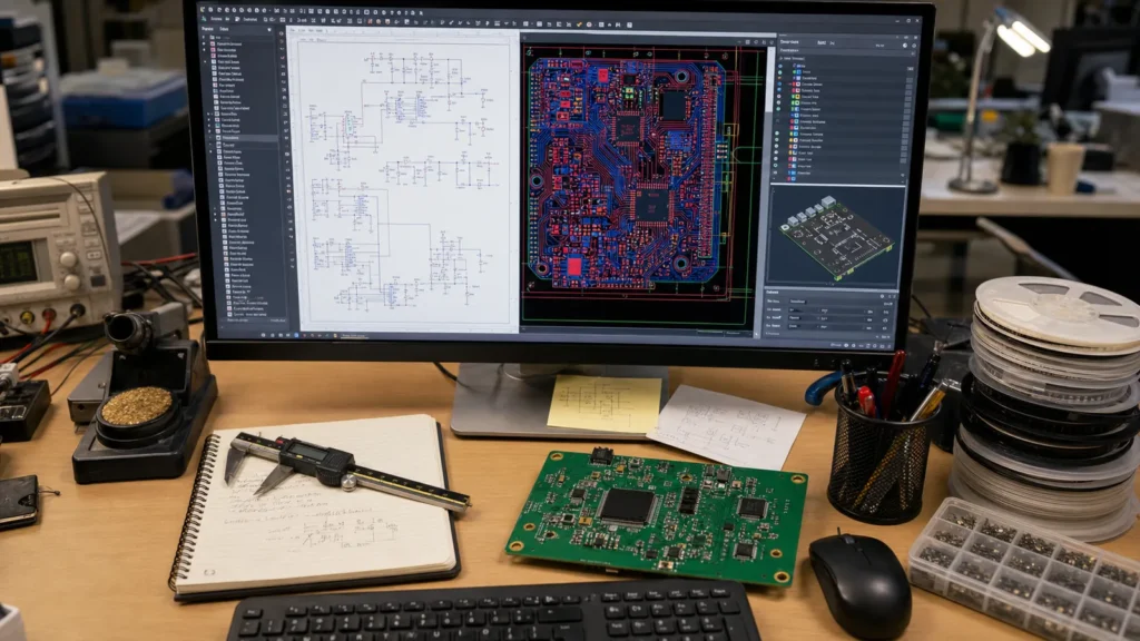
Capture schématique: dessiner un schéma logique. Ici, vous placez des symboles, des connexions câblées et attribuez des valeurs aux composants. Un bon outil de circuit gère également les feuilles hiérarchiques, les vérifications de règles de conception (DRC) et les vérifications de règles électriques (ERC).
Mise en page du PCB: Transfert du circuit sur la carte physique. L’éditeur de circuits imprimés place des traces, dirige les pistes en cuivre, définit les couches plates et applique les règles de conception pour le nettoyage, l’impédance et la fabrication.
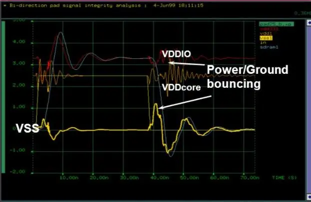
Modélisation et analyse: Simulation de SPICE pour circuits analogiques, analyse de l’intégrité du signal pour la simulation numérique à grande vitesse et l’analyse du réseau de distribution d’énergie (PDN). Ils travaillent à l’intérieur ou à côté de l’outil EDA.
résultats de production: génération de fichiers Gerber, de fichiers de forage, de données d’assemblage et d’assemblage et de dessins d’assemblage. Les erreurs à ce stade créent le rejet de la production.
Pour plus d’informations sur les pratiques schématiques, reportez-vous à. Manuel Conception de circuits imprimés PCB ReversePCB.
Plates-formes de base EDA pour la conception de circuits imprimés
Le paysage EDA est divisé en environ trois niveaux, et le choix du mauvais pour votre projet cause une véritable douleur :
| Niveaux | Outils | le mieux pour | Limites |
|---|---|---|---|
| open source / gratuit | Kicad, Easyeda, LibrePCB | Projets de loisirs, équipement ouvert, 2 à 6 couches | Simulation avancée limitée, gestion des bibliothèques moins robuste |
| professionnel de la classe moyenne | Altium Designer, OrCAD, Pads | Planches professionnelles de 4 à 16 couches, conception à grande vitesse, flux de travail d’équipe | Coût d’abonnement, courbe d’apprentissage cool |
| Entreprise / RF-Spécialisé | Cadence Allegro, Mentor Xpedition, Publicité | Multicouche complexe, RF/micro-ondes, HDI, rigide-flexible | Coût très élevé, personnel de soutien CAO spécial requis |
KICAD a comblé l’écart avec des outils de la classe moyenne pour de nombreuses conceptions. Il s’agit actuellement d’un choix professionnel viable pour les planches jusqu’à 8 niveaux si votre équipe est à l’aise de travailler avec le flux de travail de la bibliothèque. Si vous développez une carte mémoire DDR numérique haute vitesse ou plusieurs paires différentielles GHz, les outils d’intégrité Altium ou Cadence-niveau deviennent plus difficiles à remplacer.
Le flux de travail du circuit vers la carte de circuit imprimé en pratique
Voici à quoi ressemble le flux de travail EDA pour un projet de circuit imprimé typique :
Créer un diagramme. Placez des symboles, des réseaux câblés, affectez des traces et exécutez ERC pour attraper les contacts non connectés ou les sorties contradictoires.
Générer une liste de réseaux. NetList est une liste lisible par machine de chaque composant et connexion. L’outil de mise en page PCB l’importe.
Placer les composants. Placez les marques sur le contour du tableau. Regroupez les pièces associées, guidez correctement les connecteurs et laissez de la place pour les trous de montage et les zones de vitesse d’obturation.
Traces d’itinéraire. Connectez les pads en fonction de la liste des réseaux, en suivant les règles de nettoyage, les exigences de largeur de trace et les objectifs d’impédance. Les outils modernes d’EDA incluent le routage automatique, mais les réseaux critiques doivent toujours être dirigés manuellement.
Exécuter la RDC. La conception des règles de conception vérifie qu’aucune trace ne brise l’écart, qu’aucune connexion ne manque dans un seul site et que chaque réseau soit entièrement acheminé. Le passage de la RDC est l’exigence minimale avant d’envoyer la carte à la fabrication.
Générer des fichiers de production. Exportez les fichiers de forage Gerbers, NC, nomenclature et dessins d’assemblage. Vérifiez la visionneuse de Gerber – les erreurs à ce stade sont coûteuses.
Si vous passez du circuit au PCB à Altium, Ceci est Guide étape par étape Le processus complet passe.
Ce qu’il faut rechercher lors du choix d’un outil EDA
Concentrez-vous sur ce qui affecte réellement votre projet, et non sur le marketing des fonctions :
Gestion de la qualité et des bibliothèques: L’outil est-il livré avec des pistes éprouvées pour les composants que vous utilisez réellement, ou passerez-vous des heures à créer des symboles à partir de la description technique ? Une bibliothèque faible perd plus de temps que toute fonction de simulation manquante.
Possibilités de la règle de conception: Pouvez-vous définir les règles par classe net, par paire différentielle et par région ? Si vous avez besoin d’une impédance contrôlée, l’outil calcule-t-il la géométrie de la trace à partir de votre pile ?
La coopération: Plusieurs ingénieurs peuvent-ils travailler sur le même projet ? Prend-il en charge le contrôle des versions ? L’intégration de Git devient de plus en plus standard dans les outils EDA modernes.
Fiabilité de production: Est-ce que Gerber est l’exportation du conseil d’administration conformément au projet ? Certains outils appliquent silencieusement les corrections de règles de conception lors des retraits qui changent de tableau. À chaque fois, vérifiez Gerber Viewer.
Modeling integration: Si vous comptez sur la modélisation Spice, l’outil s’intégrera-t-il au départ ou avez-vous besoin d’exporter des listes de réseaux vers un simulateur externe ?
Erreurs courantes d’EDA qui atteignent la fabrication
Réseaux non rootés passant par la RDC: Certains outils permettent aux réseaux non directionnels de passer en RDC s’ils sont marqués comme « Aucune connexion ». Vérifiez visuellement chaque réseau ou avec un rapport de connexion.
Code PIN 1: Le symbole schématique et la carte de circuit imprimé ne sont pas d’accord avec l’orientation des contacts 1. C’est la cause la plus fréquente de défaillances de la première carte de révision. Vérifiez toujours visuellement les indicateurs de contact 1 visuellement sur chaque piste IC.
Silkscreen covers: sérigraphie imprimée sur des tampons en cuivre empêche la soudure. La plupart des outils ont une règle de nettoyage en sérigraphie sur le joint – allumez-le.
impédance inégalée: La géométrie de la trace dans la mise en page ne crée pas la résistance de la cible car l’outil a une définition incorrecte. Vérifiez l’impédance avec la pile du fabricant, et non l’outil par défaut.
Foire aux questions
Qu’est-ce que la conception électronique assistée par ordinateur ?
La conception électronique assistée par ordinateur (EDA) est une catégorie de logiciels utilisés pour concevoir des systèmes électroniques, incluant la saisie de schémas, le tracé de circuits imprimés (PCB), la simulation de schémas et la génération de fichiers. Les outils EDA sont indispensables au développement moderne des circuits imprimés.
KICAD est-il suffisant pour une conception de circuits imprimés professionnels ?
Oui, KiCAD est désormais capable d’imprimer un circuit imprimé de niveau professionnel pour jusqu’à 8 couches. Il prend en charge le routage de paires différentielles, le réglage long et la visualisation 3D. Pour les conceptions à grande vitesse nécessitant une modélisation avancée de l’intégrité du signal, les outils Altium ou Cadence fournissent une analyse plus approfondie.
Quelle est la différence entre la capture de schéma et la mise en page de circuits imprimés ?
La capture de schéma est une phase de conception logique dans laquelle vous définissez des connexions de composants et une fonction de schéma. La mise en page du PCB est la phase de conception physique où vous placez les composants, guidez les pistes en cuivre et préparez la carte pour la production.
Ai-je besoin de modélisation dans mon outil EDA ?
Pour les cartes numériques simples, la modélisation est facultative. Pour les circuits analogiques, les alimentations ou les conceptions numériques à grande vitesse, la modélisation des épices et l’analyse de l’intégrité du signal avant d’effectuer et de conserver les rotations.
Quels fichiers l’outil EDA génère-t-il pour la production ?
Les sorties de production standard incluent les fichiers Gerber (RS-274x ou X2) pour chaque couche de cuivre, soudure et sérigraphie ; Fichiers d’exploration CNC ; fichiers de pick-and-place (centroïde) pour la construction automatique ; et vérification des matériaux (BOM).