In the world of electronics, the term “Zero PCB” often comes up, especially among hobbyists and professionals working on custom electronic projects. But what exactly is Zero PCB technology, and how does it play a role in electronics today? In this article, we will explore the basics of Zero PCB, its applications, and why it remains a popular choice for prototyping and small-scale projects.
What is Zero PCB?
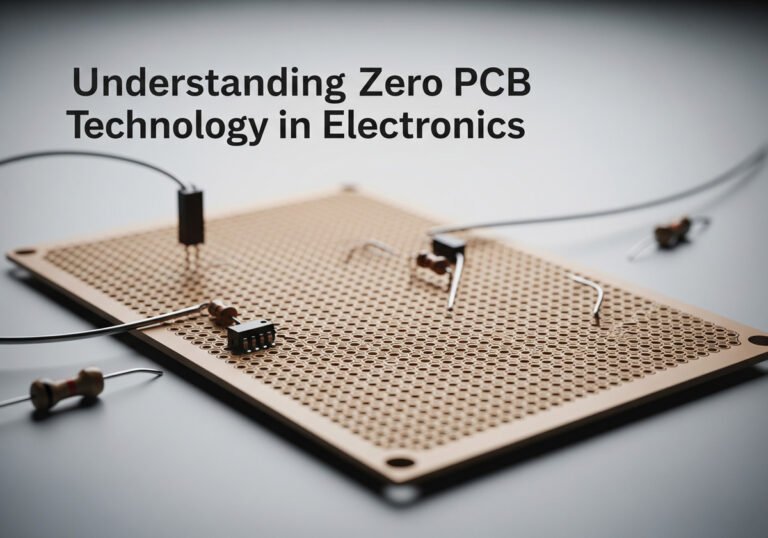
Zero PCB, also known as a “Perfboard” or “Prototype Board,” is a type of circuit board that does not have pre-defined circuit paths like a standard printed circuit board (PCB). Instead, it consists of a grid of holes, usually with a standard spacing of 0.1 inches (2.54 mm) between them. These holes are surrounded by small copper pads where components can be soldered to create custom circuits.

Unlike traditional PCBs, which are designed and manufactured with specific circuit layouts, Zero PCB offers a flexible platform for building and testing electronic circuits. This makes it an ideal choice for prototyping and experimenting with circuit designs.
Applications of Zero PCB
Prototyping and Experimentation
One of the most common uses of Zero PCB is in prototyping. Engineers and hobbyists alike use these boards to quickly assemble and test new circuit designs without the need for custom PCB fabrication. This allows for rapid iteration and experimentation, which can be especially valuable in the early stages of a project.
Educational Purposes
Zero PCB is also widely used in educational settings. Its simplicity and versatility make it an excellent tool for teaching basic electronic concepts and circuit assembly. Students can learn how to connect components, understand circuit diagrams, and gain hands-on experience in building functional circuits.
Custom Projects
For those working on custom electronics projects, Zero PCB provides the flexibility to design and build circuits tailored to specific needs. Whether it’s a one-off project or a small production run, Zero PCB allows for creative and unique circuit designs without the constraints of standardized PCBs.
Advantages of Zero PCB
Flexibility and Versatility
The primary advantage of Zero PCB is its flexibility. Since there are no pre-defined circuit paths, designers have complete freedom to create any circuit layout they desire. This is particularly beneficial for projects that require unique configurations or non-standard components.
Cost-Effectiveness
Zero PCB is generally more cost-effective than custom PCBs, especially for small projects. It eliminates the need for expensive manufacturing processes, making it an attractive option for hobbyists and small-scale productions.
Ease of Use
With its straightforward design, Zero PCB is easy to use, even for beginners. Components can be easily inserted into the holes and soldered onto the copper pads, allowing for quick assembly and modification of circuits.
Disadvantages of Zero PCB
While Zero PCB offers many benefits, there are also some drawbacks to consider:
Limited Scalability
For large-scale production, Zero PCB may not be the best option. The manual assembly process can be time-consuming and prone to errors, making it less suitable for mass production compared to automated PCB manufacturing.
Lack of Durability
Zero PCBs are typically less durable than custom-manufactured PCBs. The manual soldering process can lead to weak connections, and the absence of a protective solder mask can make the board more susceptible to damage.
Conclusion
Zero PCB technology continues to be an essential tool in the world of electronics, offering flexibility, cost-effectiveness, and ease of use for prototyping and custom projects. While it may not be suitable for large-scale production, its advantages make it an invaluable resource for hobbyists, educators, and developers.