From smartphones to high-end lighting, electronic products are becoming increasingly compact and powerful. A key contributor to this is Chip on Board (COB) technology. This report will take you on a deep dive into this revolutionary packaging method, exploring how it is reshaping the electronics manufacturing landscape.
What is COB (Chip on Board)?
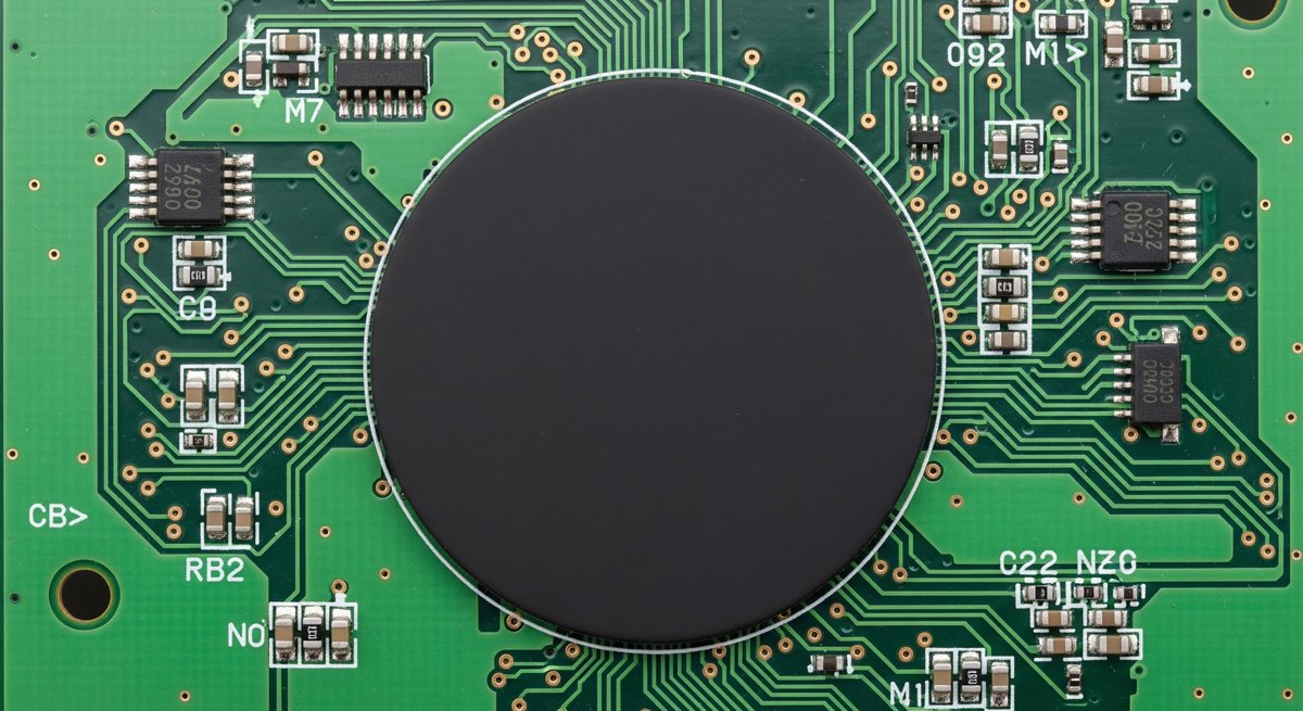
COB is an advanced electronic packaging technology that omits the traditional individual SMD chip packaging step. It directly mounts the bare semiconductor die onto a printed circuit board (PCB) or a substrate, connects it electrically using wire bonding, and then encapsulates it with resin for protection. Read more on the COB vs. SMD ultimate LED comparison.
This method significantly reduces the package size and weight, lowers manufacturing costs, and improves heat dissipation and reliability. By integrating the component and the circuit board assembly, it is also known as "level 1.5 packaging" and is a key technology for driving the miniaturization and high integration of electronic devices.
Key Advantages
-
●High Integration: Accommodates more functional chips in a smaller space, enabling device miniaturization.
-
●Excellent Heat Dissipation: Direct chip-to-substrate connection shortens the thermal path, leading to higher heat dissipation efficiency.
-
●Higher Reliability: Fewer solder joints and connection layers improve resistance to shock and vibration.
-
●Cost-Effectiveness: Simplifies the packaging process, saving on material costs.

Technical Showdown: COB vs. SMD
In the LED lighting sector, COB technology is most often compared to SMD (Surface Mount Device). As you explore their differences in key performance metrics below, consider how COB LED chips are redefining performance in a variety of applications.
How is COB Manufactured?
COB manufacturing involves a precise process. The electrical connection method for the chip is key, mainly divided into two technologies: "Wire Bonding" and "Flip-Chip."
Note: The diagrams are simplified schematics and are not drawn to scale.
A Traditional and Mature Connection Method
In this method, the die is mounted with its active face up on the substrate. Extremely thin metal wires (typically gold) are used to "stitch" the die's electrodes to the pads on the PCB, establishing an electrical connection. This is the most classic COB process.
- Pros:Mature technology, relatively low cost.
- Cons:Wires are exposed and susceptible to mechanical damage; the connection path is longer, affecting high-frequency performance and heat dissipation.
A More Advanced, Higher-Performance Option
Flip-chip technology "flips" the die, orienting its active face towards the substrate. It uses pre-fabricated solder bumps on the die to directly connect to the PCB pads, eliminating the wire bonding step.
- Pros:Shortest connection path, excellent thermal and electrical performance; no wires, higher reliability, and more compact structure.
- Cons:Higher process requirements, relatively higher cost.
Application Fields of COB Technology
With its advantages of miniaturization, high efficiency, and high reliability, COB technology has penetrated numerous high-tech fields.
LED Lighting
Achieves uniform, spot-free surface light sources, widely used in spotlights, panel lights, and high-quality linear light strips for a more comfortable lighting experience. Learn how COB LED strips are changing lighting.
Large-Scale Displays
Enables extremely small pixel pitches for higher resolution and contrast, with seamless splicing for a superior viewing experience in conference rooms, control centers, and high-end retail.
Consumer Electronics
In smartphones, smartwatches, and camera modules, COB technology integrates more sensors and processors in extremely limited space, which is critical for making devices thinner and lighter.
Automotive Electronics
Used in in-vehicle displays, Advanced Driver-Assistance Systems (ADAS) sensors, and lighting systems, meeting the strict requirements for automotive-grade reliability and compactness.
Medical Devices
In miniaturized medical devices like endoscopes and ultrasound probes, COB packaging enables high-density sensor arrays, improving diagnostic accuracy.
Communication Modules
In optical and RF modules for 5G base stations, COB technology meets the stringent demands for high frequency, high speed, low latency, and efficient heat dissipation.
Future Outlook: COB and Emerging Technologies
With the rapid development of 5G communication, the Internet of Things (IoT), and Artificial Intelligence (AI), the demand for electronic components that are miniaturized, energy-efficient, and highly reliable has reached an unprecedented level. COB technology, with its core advantages, is becoming the cornerstone that supports the development of these cutting-edge technologies. In the future, we will see COB technology in more smart devices, high-speed networks, and powerful computing centers, as it continues to drive innovation and change in the world of technology.
Conclusion
Chip on Board technology represents a significant leap forward in electronic packaging. By eliminating traditional casing, it enables devices to be smaller, more efficient, and more reliable. Its superior thermal performance and high integration capabilities position it as a critical enabler for the next generation of electronics, from miniature sensors to high-performance displays and advanced communication systems. As the demand for more powerful and compact devices continues to grow, COB will undoubtedly play an even more central role.
Frequently Asked Questions
What is the history of COB technology?
COB packaging technology evolved gradually, gaining widespread adoption in the 1960s and 1970s as a way to simplify manufacturing and lower costs by directly connecting chips to the PCB, meeting the demand for smaller, higher-performance devices.
How does COB compare to other technologies like GOB?
While COB is a true packaging technology, GOB (Glue on Board) is an enhancement to existing SMD-based displays. GOB adds a layer of glue over the surface to improve the display's moisture resistance, water resistance, and impact resistance, but it does not change the fundamental SMD packaging method.
How does COB solve heat dissipation problems?
By mounting the bare chip directly on a heat-conductive substrate, COB technology shortens the thermal path, allowing heat to dissipate much more efficiently. This helps to keep the chip's operating temperature low and enhances its longevity and performance.


