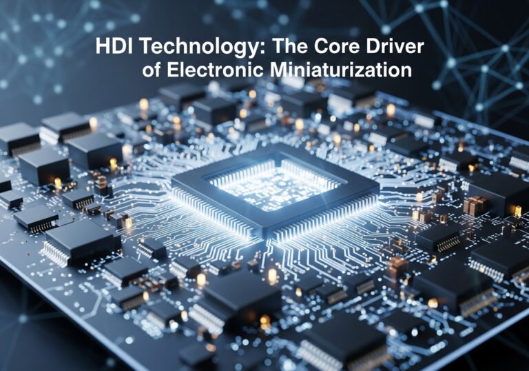
In the rapidly evolving world of electronics, the push for miniaturization is a constant. From powerful smartphones to compact wearables, the demand for smaller, more functional devices is ever-increasing. This trend has placed immense pressure on engineers to pack more components and features into shrinking spaces without compromising performance. The solution lies in High-Density Interconnect (HDI) technology, a game-changer in IC board design that enables unprecedented levels of miniaturization. HDI technology allows us to create more compact, efficient, and powerful electronic devices. This article will delve into the world of HDI technology, exploring its mechanics, key features, and pivotal role in shaping the future of smaller, more advanced IC boards.
The Basics of HDI Technology
What is HDI Technology?

Key Features Setting HDI Apart
- High Density:
The most prominent feature of HDI technology is its high density. As mentioned above, the use of micro – blind and buried – blind vias allows for a much higher density of interconnects compared to traditional PCB technology. In a traditional 4 – layer PCB, the number of available interconnection points per square centimeter might be around 100 – 200. In contrast, a first – order HDI board can have up to 500 – 800 interconnection points per square centimeter, and higher – order HDI boards can achieve even more.
- Small Aperture:
HDI boards typically have much smaller aperture sizes for their vias. While traditional PCBs may have via diameters starting from 0.3mm or more, HDI boards can have vias as small as 0.05 – 0.1mm. This reduction in via size not only increases the available space for components and wiring but also improves the electrical performance by reducing signal interference and capacitance.
- Dense Wiring:
The ability to create smaller vias and use micro – blind and buried – blind vias enables HDI boards to have much denser wiring. The line widths and spaces in HDI boards can be as small as 3 – 5 mils (1 mil = 0.0254mm), while in traditional PCBs, they are usually in the range of 8 – 12 mils. This allows for more complex circuit designs and the integration of more components in a limited space.
- Fine Lines:
HDI technology also enables the creation of fine lines on the PCB. These fine lines can carry signals more efficiently and with less interference, which is crucial for high – speed and high – frequency applications. For example, in high – speed data transmission circuits, the use of fine lines in HDI boards can help reduce signal attenuation and crosstalk.
| Feature | Traditional PCB | HDI Board |
|---|---|---|
| Via Diameter | 0.3mm - 1mm | 0.05mm - 0.1mm |
| Line Width/Spacing | 8 - 12 mils | 3 - 5 mils |
| Interconnection Points per cm² | 100 - 200 | 500 - 800 (first-order HDI, higher for higher-order) |
| Signal Integrity at High Frequencies | Lower due to larger vias and wider lines | Higher due to smaller vias and fine lines |
HDI Technology in Miniaturized IC Board Design
Enabling Smaller and More Powerful Designs
Meeting the Demands of High - Speed Signals
Applications of HDI technology
Smartphones
Smartphones are a prime example of how HDI technology has revolutionized the world of electronics. These pocket – sized powerhouses require a combination of compact design, powerful signal processing capabilities, and high – density component integration. HDI technology meets all these requirements and more.
Take, for instance, the iPhone series. Apple has been using HDI technology in its iPhones for several generations. The use of HDI boards in iPhones allows for a more compact motherboard design, which in turn enables the device to be thinner and lighter. The high – density interconnects in the HDI board ensure that the various components, such as the A – series processors, high – speed memory chips, and advanced camera modules, can communicate with each other efficiently. This results in faster data transfer speeds, better overall performance, and a seamless user experience. For example, when you’re playing a high – definition game or multitasking between multiple apps on an iPhone with an HDI – based motherboard, the smooth operation and quick response times are in part due to the capabilities of the HDI technology.
Samsung’s Galaxy S series also heavily relies on HDI technology. In these smartphones, HDI boards are used to integrate a wide range of components, including 5G modems, high – resolution displays, and advanced fingerprint sensors. The smaller vias and finer line widths in the HDI boards not only save space but also improve the signal integrity for high – speed 5G data transmission. This ensures that users can enjoy fast and stable 5G connectivity, whether they’re streaming high – definition videos, downloading large files, or engaging in real – time online gaming.
AI servers and high - performance computing
Automotive Electronics
The Manufacturing Process of HDI Circuit Boards
Step - by - Step Breakdown
The manufacturing process of HDI circuit boards is a complex and highly precise operation, involving multiple steps to achieve the high – density interconnects and miniaturized designs characteristic of these boards.
1. Raw material preparation
The manufacturing journey begins with the careful selection of raw materials. High – quality copper foils are chosen as the conductive material due to their excellent electrical conductivity. For the insulating layers, materials like FR – 4 (a type of fiberglass – reinforced epoxy laminate) or more advanced high – frequency materials are selected, depending on the specific requirements of the HDI board. These materials need to have good dimensional stability, low dielectric constant, and low dissipation factor to ensure optimal performance. For example, in high – speed applications, materials with a low dielectric constant are preferred as they reduce signal attenuation. Additionally, the pre – impregnated materials (prepregs) used to bond the layers together are also carefully sourced to ensure a strong and reliable bond.
2. Circuit diagram design and production
Engineers use specialized software, such as Altium Designer or EAGLE, to create the intricate circuit designs. This design phase is crucial as it determines the functionality and performance of the final HDI board. Once the design is complete, it is transferred to the production stage. The outer – layer circuit patterns are created through a series of processes. First, the copper – clad laminate is coated with a photoresist. Then, using a photolithography process, the circuit pattern is transferred onto the photoresist by exposing it to ultraviolet light through a mask. After exposure, the unexposed photoresist is removed through a development process. The exposed copper areas are then etched away using a chemical solution, leaving behind the desired outer – layer circuit traces.
3. Multilayer circuit board manufacturing
4. Surface treatment and testing

Challenges and Solutions in Manufacturing
The manufacturing of HDI circuit boards is not without its challenges, especially when striving for high – precision and high – quality results.
1. Precision control of laser drilling
One of the main challenges in HDI board manufacturing is achieving precise laser drilling. The small size of the vias in HDI boards requires extremely accurate drilling to ensure that the vias are located exactly where they are designed to be and have consistent diameters. Even a slight deviation in the position or diameter of the vias can lead to electrical connection problems. To address this, manufacturers use high – precision laser drilling equipment with advanced beam – control systems. These systems can precisely focus the laser beam and control its energy, reducing the chances of misalignment and inconsistent hole sizes. Additionally, continuous calibration and maintenance of the laser drilling equipment are crucial to ensure its long – term accuracy.
2. Plating Uniformity
Another significant challenge is ensuring uniform electroplating, especially in the small vias and on the fine – line traces. Inadequate plating thickness in vias can result in high – resistance connections, while over – plating can cause short circuits or other electrical issues. To achieve uniform plating, manufacturers use advanced plating techniques such as pulse plating. Pulse plating involves applying short pulses of electrical current during the plating process. This helps to deposit the metal more evenly, especially in the small vias. Specialized plating baths with carefully controlled chemical compositions are also used to ensure consistent plating quality. In addition, the design of the plating equipment, such as the use of agitation and circulation systems, helps to promote uniform distribution of the plating solution around the board, resulting in more uniform plating.
3. Layer-to-Layer Alignment
Conclusion
In short, High-Density Interconnect (HDI) technology has fundamentally reshaped the design of miniaturized IC boards. Its unique ability to create high-density, fine-line circuits has made it the backbone of modern electronics, powering everything from our smartphones to advanced AI servers and automotive systems. Despite the complexities of its manufacturing, the industry has consistently innovated to overcome challenges and refine the process.
Looking ahead, HDI technology’s role will only become more critical. As technologies like 5G, AI, and IoT continue to demand faster speeds and greater functionality in smaller packages, HDI will be instrumental in enabling these advancements. Its evolution will also align with key future trends, including the push for sustainability and the integration of even more diverse functions onto a single, compact board. Ultimately, HDI technology is not just a component of today’s electronics; it is a key driver of tomorrow’s innovations, promising smaller, faster, and more efficient devices.