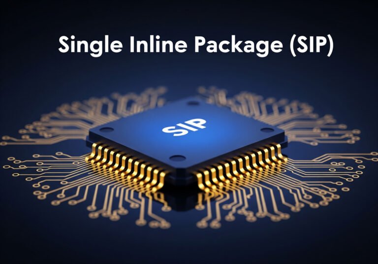
Understanding the Single Inline Package
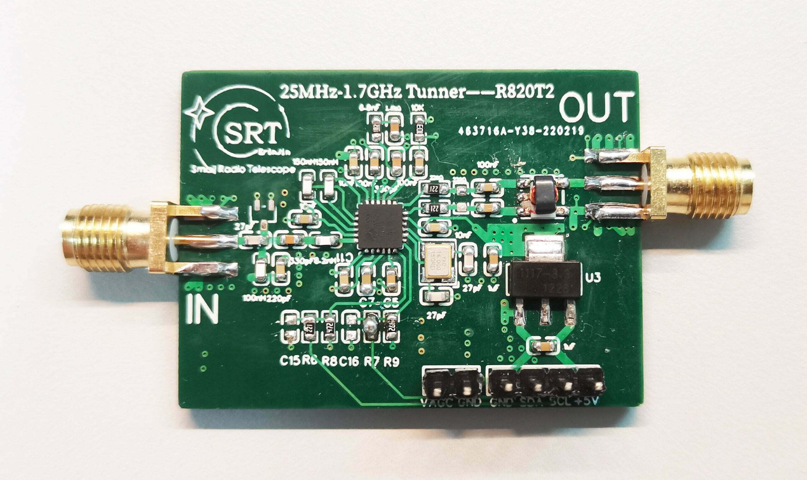
The single inline package (SIP) is a key player in electronic packaging. It offers a streamlined solution for integrated circuits. SIPs are known for their single row of connecting pins. This design makes them perfect for compact circuit layouts.
But for the abbreviation “SIP”, it can refer to multi distinct concepts in the electronics field, leading to quite a bit of confusion. We’ll explain them in next section.
Multiple Definitions of SIP
The term “Single Inline Package” (SIP) carries inherent ambiguity in the electronics world, often causing confusion among enthusiasts, students, and even professionals. This ambiguity stems from its two distinct identities: the traditional “Single-in-Line Package” — a legacy IC packaging technology — and the modern “System-in-Package” (SiP) — an advanced integration solution. Let’s break down these two concepts to clarify their roles, features, and significance.
Traditional Single-in-Line Package (SIP)
Origins and Physical Traits
- Lead count: Typically ranges from 4 to 64 pins (some sources note 2–40 pins).
- Body width: Common sizes are 300 mils or 600 mils.
- Lead pitch: Usually 100 mils.

Applications and Decline
In its heyday, traditional SIPs were widely used for packaging resistor networks, diode arrays, and small hybrid circuits like timers and oscillators. Smaller SIPs excelled in parallel-array devices, while larger ones housed more complex hybrid circuits.
However, its popularity waned due to a critical limitation: a relatively low pin count compared to alternatives like Dual-In-Line Packages (DIPs). DIPs, with their dual rows of pins, offered greater versatility for larger circuits, gradually replacing SIPs in mainstream electronics. Today, traditional SIPs are mostly found in legacy systems or niche applications, serving as a historical marker in electronics evolution.
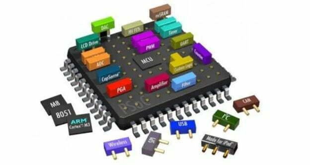
Modern System-in-Package (SiP)
Definition and Core Value
- Miniaturization: Reduces PCB footprint by 50% or more, enabling compact devices like wearables.
- Performance boost: Shorter interconnections improve electrical performance.
- Cost efficiency: Lowers engineering, assembly, and supply chain costs.
- Faster time-to-market: Streamlines design cycles and validation processes.

Manufacturing and Integration Techniques
- Heterogeneous integration: Combines components from different manufacturing processes (e.g., analog and digital chips) for optimal performance.
- Die stacking: Uses techniques like package-on-package, vertical/horizontal stacking, or embedded chips in substrates.
- Interconnection methods: Employs wire bonds, solder bumps, and flip-chip technology for reliable connections.
Enabling Technologies
- Shielding: Conformal, compartment, selective, and magnetic shielding to manage electromagnetic interference.
- Advanced packaging: Wafer-level packaging and fan-out wafer-level packaging for high-density integration.
Thermal Management
- Optimized thermal interface materials.
- Heat spreaders and integrated heat sinks.
- Design strategies like thermal vias in PCBs to dissipate heat efficiently.
Real-World Applications
- Mobile devices: Smartphones, wearables, and digital music players benefit from its compact size.
- IoT: Powers smart home sensors and smart city infrastructure.
- High-performance computing (HPC): Used in computing storage modules for AI systems.
- Automotive and aerospace: Integrated into car electronics, radar systems, and avionics.
- Medical devices: Enables compact health monitors and fitness trackers.
Other SIP Meanings Beyond Electronics
- SIPP Memory: A short-lived 30-pin memory module used in 80286 and 80386 computers. It was quickly replaced by more durable SIMMs.
- Session Initiation Protocol (SIP): A telecommunications protocol for initiating and managing voice, video, and messaging sessions (critical for VoIP services).
Comparative Analyses of Packaging Technologies
Traditional SIP vs. DIP/QFP/SOT
| Characteristic | Traditional SIP | DIP | QFP | SOT |
|---|---|---|---|---|
| Form Factor | Single row of leads | Dual rows of leads | Quad flat, no leads | Small outline, 3-6 leads |
| Pin Count | 2–64 | 4–64+ | 32–304+ | 3–6 |
| Mounting Technology | Through-hole | Through-hole/surface-mount | Surface-mount | Surface-mount |
| Typical Applications | Resistor networks, legacy systems | General ICs, microcontrollers | Complex ICs (microprocessors) | Transistors, small ICs |

SiP vs. SoC
| Characteristic | SiP | SoC |
|---|---|---|
| Integration Level | Multiple dies in one package | Single semiconductor die |
| Flexibility | Mixes components from different processes | Limited by single process node |
| Cost | Lower NRE, ideal for mid-volume | High NRE, optimized for high volume |
| Performance | Excellent (short interconnections) | Highest (on-die interconnects) |
| Applications | Mobile, IoT, automotive | High-volume consumer electronics (e.g., smartphone CPUs) |
SiP vs. MCM
| Characteristic | SiP | MCM |
|---|---|---|
| Evolution | Evolved from MCM, adds die stacking | Predecessor to SiP, no die stacking |
| Integration Density | Higher (stacked dies) | Moderate (side-by-side chips) |
| Manufacturing | Uses advanced packaging (wafer-level) | Often uses simpler processes |
| Applications | Compact systems (wearables, IoT) | Telecommunications, high-speed data processing |
Choosing the Right Package Solution for Your Project
Selecting the right package solution for an electronic project is crucial. The choice affects performance, size, and cost. Single Inline Packages (SIPs) present a viable option for many projects.
When considering SIPs, evaluate your project’s space constraints. SIPs are ideal when circuit board space is tight. Their inline design maximizes usage while maintaining efficiency.
Cost is another factor to weigh. SIPs are often cost-effective, especially for small-scale production. Their simplicity in design and manufacturing reduces expenses.
However, not all projects will fit SIPs. Consider the number of connections needed in your circuit. SIPs may not suit applications that need many pin connections, where another packaging type might be more appropriate.