PCB Design Cases
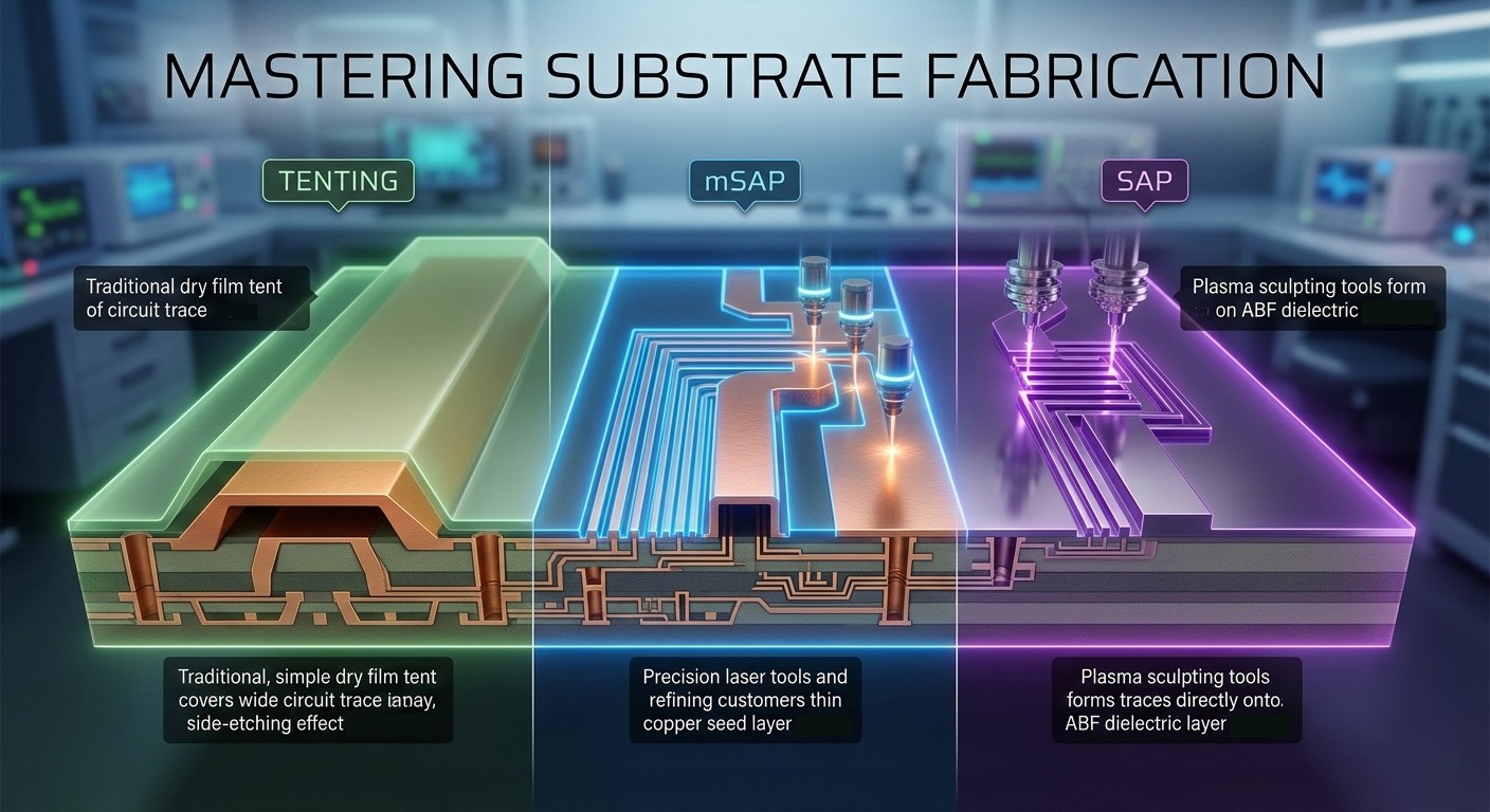
Comparing Tenting, mSAP, and SAP Process in PCB Substrate Fabrication
A technical comparison of Tenting, mSAP, and SAP processes in high-end PCB substrate fabrication. Explore how these methods solve side-etching issues and enable sub-10μm line precision for AI and 5G chips.
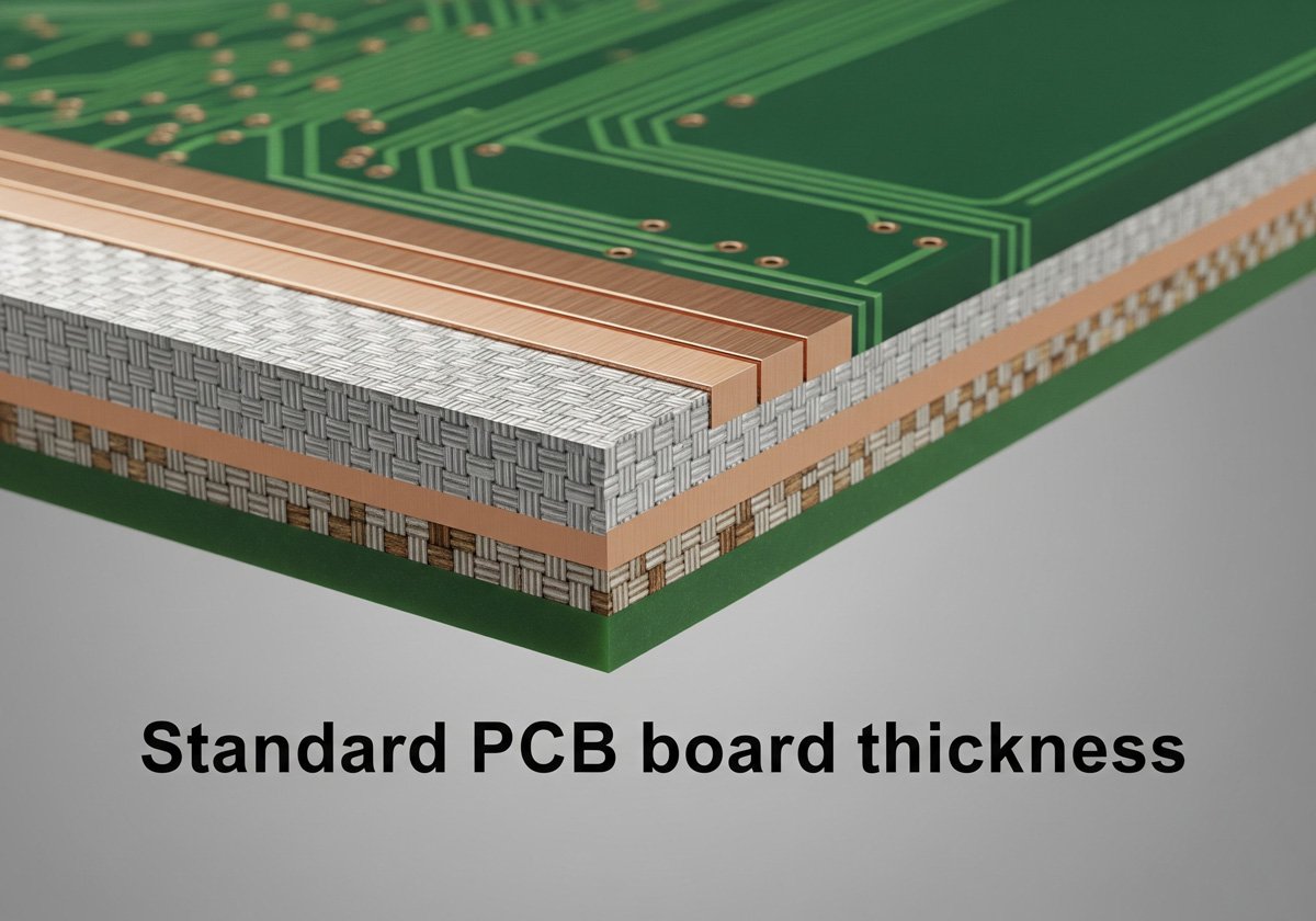
Standard PCB Board Thickness
A comprehensive guide to standard PCB board thickness. Learn its impact on mechanical stability & electrical performance, and choose the right one for your projects.

Achieving EMC Compliance in Complex PCB Layouts
Achieving EMC compliance in complex PCB designs requires a comprehensive approach, from strategic layout and robust grounding to advanced simulation and rigorous testing.

The Role of HDI Technology in Miniaturized IC Board Design
In the rapidly evolving world of electronics, the push for miniaturization is a constant. From powerful smartphones to compact wearables, the demand for smaller, more functional devices is ever-increasing. This

Advanced Routing Techniques for High-Speed IC Boards
High-speed IC boards power today’s tech, from 5G gear to supercomputers. Routing—how signals travel—makes or breaks performance. This post dives into advanced techniques, focusing on signal integrity, design, protocols, and

Choosing the Right EDA Software for Your IC Board Design Project
In the dynamic and complex realm of Integrated Circuit (IC) board design projects, the choice of Electronic Design Automation (EDA) software stands as a linchpin for success. EDA software has
The Complete Guide to IC Board Design
In the realm of modern electronics, Integrated Circuit (IC) board design stands as a cornerstone technology, playing a pivotal role in the creation of a vast array of devices that

Electronic Manufacturing Services: A Comprehensive Guide
Explore the ins and outs of electronic manufacturing services, including contract manufacturing and supply chain management, to streamline production and cut costs efficiently.


