STM32F030 Chip Introduction
The STM32F030 chip is a low-cost, 32-bit ARM Cortex-M0 microcontroller from STMicroelectronics. It features up to 32KB of Flash and 4KB of SRAM, and can run at up to 48MHz. It includes a variety of peripherals, such as analog comparators, timers, and I2C and SPI interfaces. The STM32F030 also supports motor control applications, and it has a wide range of integrated analog and digital peripherals. The chip’s small size and low power consumption make it ideal for use in a variety of applications, from consumer electronics to medical and industrial systems. The chip’s price and performance make the STM32F030 a great choice for cost-conscious developers. With support for a variety of development tools, including STM32Cube and the STM32CubeMX graphical configuration tool, it’s easy to get up and running with the STM32F030 and develop innovative applications.
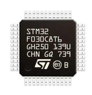
Parameters
– CPU: ARM Cortex-M0 core with 32-bit RISC architecture
– Operating frequency: up to 48 MHz
– Program memory: up to 32KB Flash
– RAM: up to 4KB
– Clock source: Internal 8MHz or external 32kHz
– Clock output: 2 x 32 kHz
– Digital I/O: Up to 36 I/O pins
– Analog inputs: Up to 8 x 12-bit ADC channels
– Timers: Up to 3 x 16-bit timers
– Communication interfaces: Up to 2 x I2C, 2 x USART, SPI, CAN
System Architecture
The internal system framework of STM32F030 can be simply divided into 2 master and 4 slave systems. The master and slave concepts here are relative to Busmatrix:
- Masters
- Cortex-M0 core AHB bus
- GP-DMA
- Slaves
- Internal SRAM
- Internal Flash
- AHB2APB
- AHB to GPIO ports
The relationship between 2 masters and 4 slaves is shown in the following figure in more detail and marked:
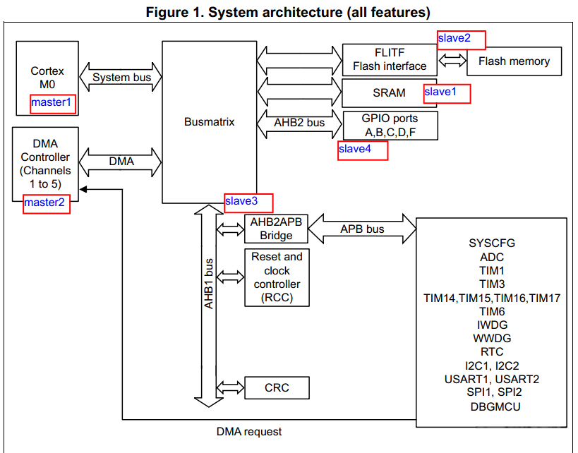
For the AHB2APB Bridge, if you want to use the peripherals connected to the APB bus, you must call a register such as RCC_AHBENR to enable the peripheral clock first, and the peripheral is the peripheral driver. These details are generally handled in the ST driver API.
Memory Overview
In the STM32F030 program, data, registers, and IO ports are all mapped to the 4GB address space (32-bit machine). The memory map of the STM32F030 is detailed in the datasheet.
SRAM
The STM32F030 SRAM has a size of 8KB and can be accessed in byte, word, and half-word units. This section is used to store the compiled and linked code, data, and program stack during runtime. Data is constantly read from or written to this SRAM during program execution.
Flash
The internal flash of the STM32F030 is usually sufficient for use as it is designed for this purpose. It has 64KB of user flash space. Flash inside the chip is referred to as internal flash or ROM (ROM and flash differ in that ROM cannot be erased by the user and is fixed during chip production, whereas flash can be erased and rewritten at any time).
The internal flash of the STM32F030 is divided into two types:
- 64KB of user flash space: used to download the .bin code generated by the user’s compilation and linking.
- Info flash: includes option bytes and system memory.
Option bytes can be used to configure some functions of the IC.
System memory is the IC’s memory, which contains a code segment fixed during IC production that is not open source and whose operation can only be guessed. The purpose of system memory is to act as an embedded bootloader. Generally, it is not used for debugging. The typical usage is to connect a debugger through an SWD interface to the IC and easily download and debug the code. However, for products, the SWD interface may not be exposed. In this case, the product’s .bin code can be downloaded and run through the IC’s internal system memory bootloader via a serial interface, which is the typical process for firmware updates. STM will provide the interface and usage demo for the system memory bootloader, and there are many related documentation explaining how to use it.
Boot Configuration
Debugging through SWD is called “system programming,” while loading and starting programs using a bootloader is considered “application programming.” STM has three configurable boot modes for different application scenarios.
Boot mode configuration:
Firstly, there is a boot pin that connects to high or low levels. When the chip starts up, it checks the boot pin level and switches to the corresponding boot mode. In addition, nBOOT1 can be configured in the option byte to select the corresponding boot mode.
Classification of boot modes:
There are three types: User flash boot, which is the most common; after compiling and linking, download the code, reset, and run your own flash code. System memory boot, which uses the IC’s internal bootloader to boot. SRAM boot.
Clock Frame
The clock frame of STM32F030 is as follows, and here are some definitions of them:
- HSI: called high-speed internal clock, is composed of RC oscillator.
- HSE: called a high-speed external clock, can be connected to an external quartz/ceramic resonator, or an external clock source.
- LSI: called a low-speed internal clock, composed of an RC oscillator, has a low frequency, and the STM32F030 is 40kHz.
- LSE: called a low-speed external clock, generally connected with a quartz crystal with an external frequency of 32.768kHz.
- PLL: is the multiplier output of the phase-locked loop.
- HSI14 RC: clock source can be used for ADC alone.
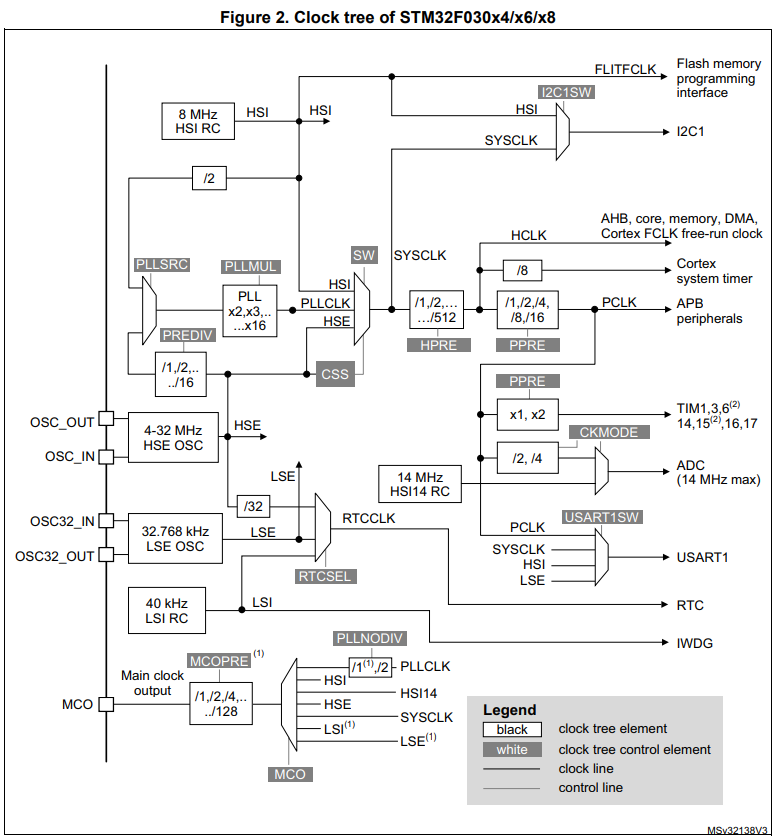
Peripherals that are not specifically stated generally use PCLK. Here is a brief list of the situations that need to be enabled with AHB/APB according to the specific code:
- Use AHB as clock source: GPIOA-F, TS, CRC, FLITF, SRAM, DMA1.
- Use APB1 as clock source: TIM2, TIM3, TIM6, TIM14, WWDG, SPI2, USART2, I2C1, I2C2, PWR, DAC, CEC.
- Use APB2 as the clock source: SYSCFG, ADC1, TIM1, SPI1, USART1, TIM15, TIM16, TIM17, DBGMCU.
Reset Function
Reset is a crucial part of the MCU system startup process. When the IC starts executing the program, it begins from the reset, which is the first step after the system is powered on.
Reset Mechanism of Cortex-M0
In the startup file of Cortex-M0, you will always see the reset_handler, which is located at the first position of the vector table. The address of Cortex-M0 is 0x0000 0004, and the PC value when Cortex-M0 starts working is this address. In the reset_handler, the user’s implemented SystemInit function is generally called, which sets up the clock of the various components needed by the system to work correctly, making it easier for the system to operate normally later on. Then, the __main entry in the library is called, which should perform some initial processing of the C runtime library and set up the stack.
Types of Reset
There are three main types of reset for STM32F030: Power reset, System reset, and RTC domain reset.
Power reset is related to the power supply of the IC. This reset is triggered by power-on and wake-up from standby, and the system initialization starts after the reset.
System reset is triggered by the system. That is, the power supply is normal, but if the reset button is pressed, the corresponding register is reset by software, or the Watchdog is triggered, this reset will occur. When this reset occurs, the only difference from the power reset is that the relevant bit in the RCC_CSR register used to indicate the reset source will not be reset, while all other registers will be reset to the state just after power-on.
The trigger of the RTC domain reset is also a software trigger. It is triggered by writing to the corresponding bit in the RCC_BDCR register. However, this type of reset only affects the RTC and LSE crystal, etc.
CRC
CRC, the Cyclic Redundancy Check, is a check algorithm that checks the integrity of transmitted/stored data. Because it may be used in many places, STM32F030 implements this algorithm with a CRC hardware computing unit in the IC. When an application needs to use CRC, then the hardware unit can be controlled by software to realize the requirements (of course CRC can also be implemented in software, but the speed is definitely not as fast as hardware CRC).
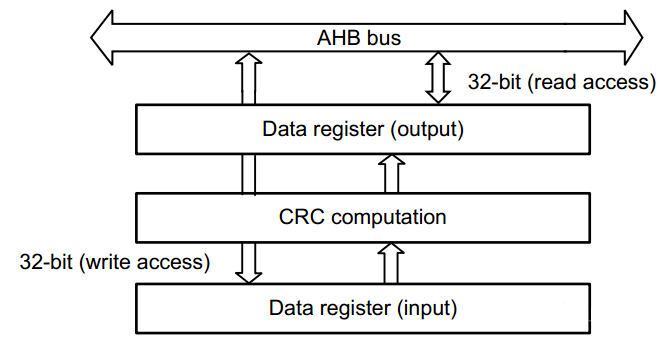
The CRC process is implemented inside the IC, so you only need to know how to use it, and it is very simple to use. Write the source data that needs to be calculated from the Data register (input), start the calculation of the CRC calculation unit, and then read the calculated results in the Data register (output).
In fact, the input and output of the CRC Data register of the STM32F030 use the same register, because it must be input first, and then the output can be obtained before continuing to the next input. It can be seen from this process that the input and output are not used at the same time, so you can directly use a register to multiplex the two functions. The register can be operated in 32 bit, 16 bit, 8 bit, which can meet different requirements.
STM32F030 Development Board - STM32f0308 Discovery
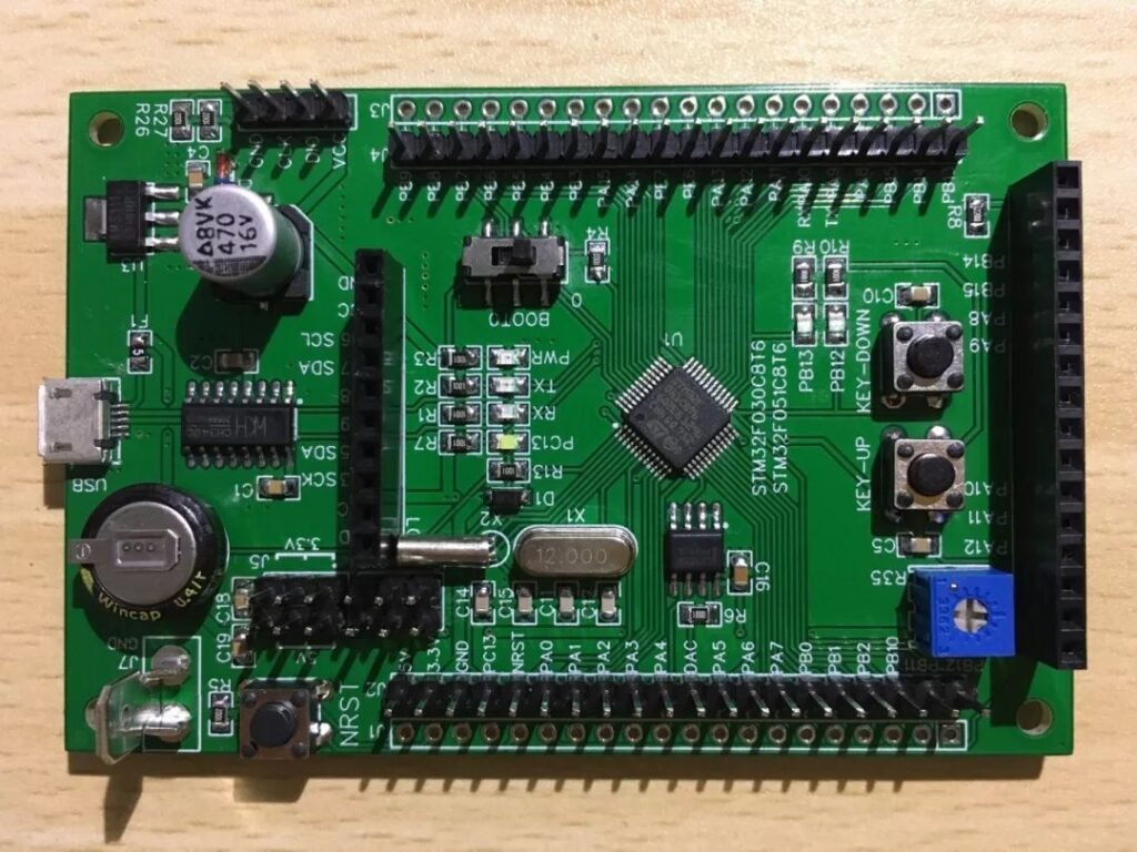
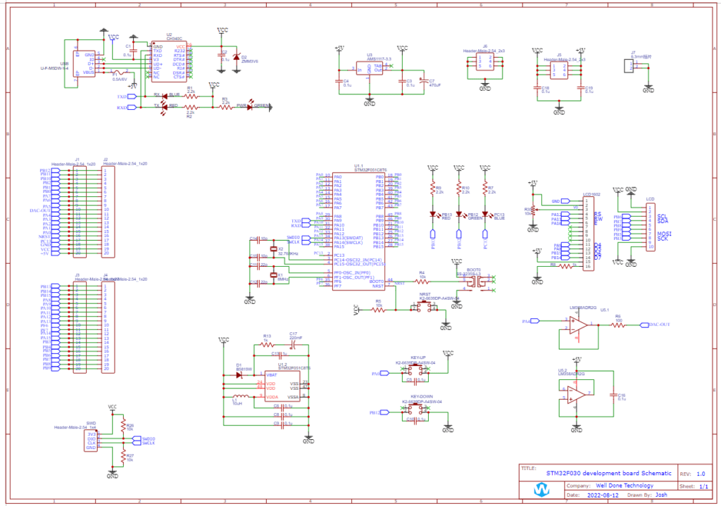
The development of this STM32F030 microcontroller is based on the latest HAL library of STM32, the initialization code generated by STM32CubeMX, and its compiler is GCC. Below is its schematic, pcb diagram and assembled board. STM32 provides many entry-level development boards, such as the Discovery series and the Nucleo series. The stm32f0308 discovery is one of the boards in the Discovery series, which is equipped with the STM32F030 chip.
The basic functions and features of the Discovery series development boards are similar, but the capabilities of the accompanying chips may vary. The features of the stm32f0308 discovery are as follows:
Convenient IO port extension: With just one USB cable connected to a PC, development can be carried out. The IO ports of the STM32F030 chip on the development board are extended, making it easy to connect to different devices using DuPont wires.
Debugging interface: The development board comes with an onboard SWD debug interface, which is implemented using another Cortex-M3 chip from ST (currently, the v9 version of JLINK on the market should also be using ST’s Cortex-M3 chip). This SWD debug interface can be used separately through the connection of a jumper cap, which means that the stm32f0308-discovery can be used as a standalone SWD debugger.
Flexible power supply: The development board itself is powered by USB, but it has a voltage conversion circuit that can output 5V and 3V power supplies for external devices to use (note that the power supply current is still limited). Generally, small modules and interfaces can be powered directly by it.
Board-level peripherals: Since it is an entry-level, low-cost development board, the onboard peripherals are very simple, consisting of two buttons and four LEDs. Of the two buttons, one is used for reset and the other is a user-programmable button. Of the four LEDs, one is a power indicator, one is an SWD debug status indicator, and the remaining two can be programmed for control. So, in reality, the onboard peripherals that can be programmed for control are just one user button and two user LEDs.
Performance
- Reserved SWD interface for debugging by ST-LINK;
- The PA4 (DAC output) interface with high port drive capability;
- Two light touch buttons and 3 LEDs for easy debugging;
- LCD1602 interface and an interface compatible with common TFT LCD;
- Use a supercapacitor as an RTC backup power supply;
- USB interface with power protection;
- Multiple power supply test points for oscilloscope or multimeter.

